ADC1001CCJ-1 National Semiconductor, ADC1001CCJ-1 Datasheet - Page 3
ADC1001CCJ-1
Manufacturer Part Number
ADC1001CCJ-1
Description
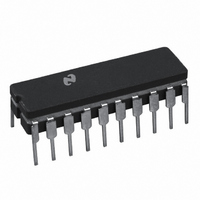
IC ADC 10BIT MPU COMPAT 20-CDIP
Manufacturer
National Semiconductor
Datasheet
1.ADC1001CCJ.pdf
(9 pages)
Specifications of ADC1001CCJ-1
Number Of Bits
10
Sampling Rate (per Second)
4.6k
Data Interface
Parallel
Number Of Converters
1
Voltage Supply Source
Single Supply
Operating Temperature
0°C ~ 70°C
Mounting Type
Through Hole
Package / Case
20-CDIP (0.300", 7.62mm)
Lead Free Status / RoHS Status
Contains lead / RoHS non-compliant
Other names
*ADC1001CCJ-1
Available stocks
Company
Part Number
Manufacturer
Quantity
Price
Company:

Part Number:
ADC1001CCJ-1
Manufacturer:
AD
Quantity:
88


CONTROL INPUTS [Note: CLK IN is the input of a Schmitt trigger circuit and is therefore specified separately]
V
V
I
I
CLOCK IN
V
V
V
OUTPUTS AND INTR
V
V
I
I
I
POWER SUPPLY
I
IN
IN
OUT
SOURCE
SINK
CC
The following specifications apply for V
IN
IN
T
T
H
OUT
OUT
DC Electrical Characteristics
Symbol
Note 1: Absolute Maximum Ratings indicate limits beyond which damage to the device may occur. DC and AC electrical specifications do not apply when operating
the device beyond its specified operating conditions.
Note 2: All voltages are measured with respect to GND, unless otherwise specified. The separate A GND point should always be wired to the D GND.
Note 3: A zener diode exists, internally, from V
Note 4: For V
for analog input voltages one diode drop below ground or one diode drop greater than the V
level analog inputs (5V) can cause this input diode to conduct — especially at elevated temperatures, and cause errors for analog inputs near fullscale. The spec al-
lows 50 mV forward bias of either diode. This means that as long as the analog V
be correct. To achieve an absolute 0 V
tolerance and loading.
Note 5: With an asynchronous start pulse, up to 8 clock periods may be required before the internal clock phases are proper to start the conversion process. The
start request is internally latched, see Figure 3 .
Note 6: The CS input is assumed to bracket the WR strobe input and therefore timing is dependent on the WR pulse width. An arbitrarily wide pulse width will hold
the converter in a reset mode and the start of conversion is initiated by the low to high transition of the WR pulse (see Timing Diagrams).
Note 7: All typical values are for T
Note 8: Accuracy is guaranteed at f
Note 9: The V
of these two equal resistors.
Note 10: Human body model, 100 pF discharged through a 1.5 k
+
−
(1)
(0)
(1)
(0)
(0)
(1)
IN
REF/2
Logical “1” Input Voltage
(Except CLK IN)
Logical “0” Input Voltage
(Except CLK IN)
Logical “1” Input Current
(All Inputs)
Logical “0” input Current
(All Inputs)
CLK IN Positive Going
Threshold Voltage
CLK IN Negative Going
Threshold Voltage
CLK IN Hysteresis
(V
Logical “0” Output Voltage
Logical “1” Output Voltage
TRI-STATE Disabled Output
Leakage (All Data Buffers)
Supply Current (Includes
Ladder Current)
(−) V
T
+)−(V
pin is the center point of a two resistor divider (each resistor is 2.4k ) connected from V
IN
(+) the digital output code will be all zeros. Two on-chip diodes are tied to each analog input (see Block Diagram) which will forward conduct
T
−)
Parameter
A
= 25˚C.
CLK
DC
= 410 kHz. At higher clock frequencies accuracy can degrade.
to 5 V
DC
CC
CC
input voltage range will therefore require a minimum supply voltage of 4.950 V
to GND and has a typical breakdown voltage of 7 V
= 5 V
DC
V
V
V
V
I
I
I
V
V
V
V
f
V
and CS = 1
OUT
O
O
CLK
and T
CC
CC
IN
IN
OUT
OUT
OUT
OUT
REF
= −360 µA, V
= −10 µA, V
= 5 V
= 0 V
= 5.25 V
= 4.75 V
= 410 kHz,
= 1.6 mA, V
/2 = NC, T
resistor.
= 0.4 V
= 5 V
Short to GND, T
Short to V
MIN
DC
DC
DC
Conditions
T
DC
DC
DC
A
CC
A
CC
3
T
= 25˚C
CC
IN
= 4.75 V
CC
MAX
= 4.75 V
does not exceed the supply voltage by more than 50 mV, the output code will
= 4.75 V
, T
, unless otherwise specified.
A
A
= 25˚C
= 25˚C
CC
DC
DC
DC
supply. Be careful, during testing at low V
DC
.
CC
MIn
2.0
2.7
1.5
0.6
2.4
4.5
4.5
9.0
−1
to ground. Total ladder input resistance is the sum
−0.005
0.005
Typ
3.1
1.8
1.3
0.1
0.1
2.5
16
DC
6
over temperature variations, initial
CC
−100
Max
levels (4.5V), as high
0.8
3.5
2.1
2.0
0.4
5.0
15
1
3
www.national.com
mA
mA
Units
µA
µA
µA
µA
V
V
V
V
V
V
V
V
mA
DC
DC
DC
DC
DC
DC
DC
DC
DC
DC
DC
DC
DC
DC
Related parts for ADC1001CCJ-1
Image
Part Number
Description
Manufacturer
Datasheet
Request
R

Part Number:
Description:
ADC1001 - 10-Bit µP Compatible A/D Converter, Package: Cerdip, Pin Nb=20
Manufacturer:
National Semiconductor Corporation
Datasheet:

Part Number:
Description:
National Semiconductor [8-Bit D/A Converter]
Manufacturer:
National Semiconductor
Datasheet:
Part Number:
Description:
National Semiconductor [Media Coprocessor]
Manufacturer:
National Semiconductor
Datasheet:
Part Number:
Description:
Digitally Controlled Tone and Volume Circuit with Stereo Audio Power Amplifier, Microphone Preamp Stage and National 3D Sound
Manufacturer:
National Semiconductor
Datasheet:
Part Number:
Description:
Digitally Controlled Tone and Volume Circuit with Stereo Audio Power Amplifier, Microphone Preamp Stage and National 3D Sound
Manufacturer:
National Semiconductor
Datasheet:
Part Number:
Description:
AC97 Rev 2 Codec with Sample Rate Conversion and National 3D Sound
Manufacturer:
National Semiconductor
Part Number:
Description:
Manufacturer:
National Semiconductor
Datasheet:
Part Number:
Description:
Manufacturer:
National Semiconductor
Datasheet:
Part Number:
Description:
General Purpose, Low Voltage, Low Power, Rail-to-Rail Output Operational Amplifiers
Manufacturer:
National Semiconductor
Datasheet:
Part Number:
Description:
8-bit 20 MSPS flash A/D converter.
Manufacturer:
National Semiconductor
Datasheet:
Part Number:
Description:
Low Noise Quad Operational Amplifier
Manufacturer:
National Semiconductor
Datasheet:
Part Number:
Description:
Quad Differential Line Receivers
Manufacturer:
National Semiconductor
Datasheet:
Part Number:
Description:
Quad High Speed Trapezoidal? Bus Transceiver
Manufacturer:
National Semiconductor
Datasheet:
Part Number:
Description:
Dual Line Receiver
Manufacturer:
National Semiconductor
Datasheet: