ADC1001CCJ-1 National Semiconductor, ADC1001CCJ-1 Datasheet - Page 2
ADC1001CCJ-1
Manufacturer Part Number
ADC1001CCJ-1
Description
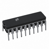
IC ADC 10BIT MPU COMPAT 20-CDIP
Manufacturer
National Semiconductor
Datasheet
1.ADC1001CCJ.pdf
(9 pages)
Specifications of ADC1001CCJ-1
Number Of Bits
10
Sampling Rate (per Second)
4.6k
Data Interface
Parallel
Number Of Converters
1
Voltage Supply Source
Single Supply
Operating Temperature
0°C ~ 70°C
Mounting Type
Through Hole
Package / Case
20-CDIP (0.300", 7.62mm)
Lead Free Status / RoHS Status
Contains lead / RoHS non-compliant
Other names
*ADC1001CCJ-1
Available stocks
Company
Part Number
Manufacturer
Quantity
Price
Company:

Part Number:
ADC1001CCJ-1
Manufacturer:
AD
Quantity:
88


www.national.com
Linearity Error
Zero Error
Full-Scale Error
Total Ladder Resistance (Note 9)
Analog Input Voltage Range
DC Common-Mode Error
Power Supply Sensitivity
T
f
CR
t
t
t
t
t
C
C
CLK
W(WR)L
ACC
1H
WI
1rs
Converter Specifications: V
Timing Specifications: V
c
IN
OUT
Converter Characteristics
AC Electrical Characteristics
Absolute Maximum Ratings
If Military/Aerospace specified devices are required,
please contact the National Semiconductor Sales Office/
Distributors for availability and specifications.
Supply Voltage (V
Logic Control Inputs
Voltage at Other Inputs and Outputs
Storage Temperature Range
Package Dissipation at T
Symbol
, t
, t
RI
0H
Parameter
Conversion Time
Clock Frequency
Clock Duty Cycle
Conversion Rate In Free-Running
Mode
Width of WR Input (Start Pulse
Width)
Access Time (Delay from
Falling Edge of RD to Output
Data Valid)
TRI-STATE
from Rising Edge of RD to
Hi-Z State)
Delay from Falling Edge
of WR or RD to Reset of INTR
INTR to 1st Read Set-Up Time
Input Capacitance of Logic
Control Inputs
TRI-STATE Output
Capacitance (Data Buffers)
CC
) (Note 3)
A
CC
®
= 25˚C
Parameter
Control (Delay
= 5 V
CC
= 5 V
DC
and T
DC
, V
Input Resistance at Pin 9
(Note 4) V(+) or V(−)
Over Analog Input Voltage Range
V
Allowed V
Voltage Range (Note 4)
−0.3V to (V
CC
A
REF
= 25˚C unless otherwise specified.
−65˚C to +150˚C
= 5 V
/2 = 2.500 V
−0.3V to +18V
(Notes 1, 2)
DC
IN
±
CC
(+) and V
875 mW
Conditions
5% Over
+0.3V)
(Note 5)
f
(Note 8)
INTR tied to WR with
CS = 0 V
CS = 0 V
C
C
(See TRI-STATE Test
Circuits)
CLK
6.5V
DC
L
L
= 100 pF
= 10 pF, R
, T
= 410 kHz
IN
MIN
(−)
2
Conditions
DC
DC
T
, f
Lead Temp. (Soldering, 10 seconds)
ESD Susceptibility (Note 10)
Operating Conditions
Temperature Range
Range of V
(Note 6)
A
L
CLK
= 10k
ADC1001CCJ
ADC1001CCJ-1
T
MAX
= 410 kHz
and f
CC
CLK
GND−0.05
MIn
= 410 kHz unless otherwise specified.
2.2
MIn
195
100
150
550
80
40
Typ
±
±
4.8
Typ
1
1
170
125
300
400
⁄
⁄
8
8
5
5
(Notes 1, 2)
V
CC
1260
4600
4.5 V
Max
Max
220
300
200
450
7.5
7.5
±
±
±
90
60
+0.05
−40˚C T
1
2
2
T
0˚C T
MIN
DC
to 6.3 V
T
A
A
A
conv/s
1/f
Units
+85˚C
+70˚C
Units
kHz
300˚C
pF
pF
LSB
LSB
LSB
LSB
LSB
µs
ns
ns
ns
ns
ns
V
%
800V
T
K
CLK
MAX
DC
DC
Related parts for ADC1001CCJ-1
Image
Part Number
Description
Manufacturer
Datasheet
Request
R

Part Number:
Description:
ADC1001 - 10-Bit µP Compatible A/D Converter, Package: Cerdip, Pin Nb=20
Manufacturer:
National Semiconductor Corporation
Datasheet:

Part Number:
Description:
National Semiconductor [8-Bit D/A Converter]
Manufacturer:
National Semiconductor
Datasheet:
Part Number:
Description:
National Semiconductor [Media Coprocessor]
Manufacturer:
National Semiconductor
Datasheet:
Part Number:
Description:
Digitally Controlled Tone and Volume Circuit with Stereo Audio Power Amplifier, Microphone Preamp Stage and National 3D Sound
Manufacturer:
National Semiconductor
Datasheet:
Part Number:
Description:
Digitally Controlled Tone and Volume Circuit with Stereo Audio Power Amplifier, Microphone Preamp Stage and National 3D Sound
Manufacturer:
National Semiconductor
Datasheet:
Part Number:
Description:
AC97 Rev 2 Codec with Sample Rate Conversion and National 3D Sound
Manufacturer:
National Semiconductor
Part Number:
Description:
Manufacturer:
National Semiconductor
Datasheet:
Part Number:
Description:
Manufacturer:
National Semiconductor
Datasheet:
Part Number:
Description:
General Purpose, Low Voltage, Low Power, Rail-to-Rail Output Operational Amplifiers
Manufacturer:
National Semiconductor
Datasheet:
Part Number:
Description:
8-bit 20 MSPS flash A/D converter.
Manufacturer:
National Semiconductor
Datasheet:
Part Number:
Description:
Low Noise Quad Operational Amplifier
Manufacturer:
National Semiconductor
Datasheet:
Part Number:
Description:
Quad Differential Line Receivers
Manufacturer:
National Semiconductor
Datasheet:
Part Number:
Description:
Quad High Speed Trapezoidal? Bus Transceiver
Manufacturer:
National Semiconductor
Datasheet:
Part Number:
Description:
Dual Line Receiver
Manufacturer:
National Semiconductor
Datasheet: