ADC1001CCJ-1 National Semiconductor, ADC1001CCJ-1 Datasheet
ADC1001CCJ-1
Specifications of ADC1001CCJ-1
Available stocks


Related parts for ADC1001CCJ-1


ADC1001CCJ-1 Summary of contents
Page 1
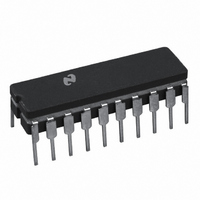
... Operates ratiometrically or with bits analog span adjusted voltage reference ± 1 LSB n 0.3" standard width 20-pin DIP package 200µS ADC1001 Dual-In-Line Package DS005675-11 Top View 0˚C to +70˚C −40˚C to +85˚C ADC1001CCJ-1 ADC1001CCJ J20A J20A June 1999 , 2 www.national.com ...
Page 2
... Control Inputs C TRI-STATE Output OUT Capacitance (Data Buffers) www.national.com (Notes 1, 2) Lead Temp. (Soldering, 10 seconds) ESD Susceptibility (Note 10) Operating Conditions 6.5V Temperature Range −0.3V to +18V ADC1001CCJ −0. +0.3V) ADC1001CCJ-1 CC −65˚C to +150˚C Range 875 2.500 and f REF DC MIN A MAX CLK Conditions GND− ...
Page 3
DC Electrical Characteristics = 5 V The following specifications apply for V CC Symbol Parameter CONTROL INPUTS [Note: CLK IN is the input of a Schmitt trigger circuit and is therefore specified separately] V (1) Logical “1” Input Voltage IN ...
Page 4
Typical Performance Characteristics Logic Input Threshold Voltage vs Supply Voltage DS005675-14 Output Current vs Temperature DS005675-17 TRI-STATE Test Circuits and Waveforms DS005675-5 www.national.com Delay From Falling Edge Output Data Valid vs Load Capacitance DS005675-15 DS005675 ...
Page 5
TRI-STATE Test Circuits and Waveforms Timing Diagrams *All timing is measured from the 50% voltage points. (Continued) Output Enable and Reset INTR 5 DS005675-7 DS005675-8 www.national.com ...
Page 6
Timing Diagrams (Continued) Byte Sequencing For The 20-Pin ADC1001 Byte 8-Bit Data Bus Connection Order DB7 DB6 DB5 MSB 1st Bit 9 Bit 8 Bit 7 LSB 2nd Bit 1 Bit 0 0 Functional Description The ADC1001 uses an advanced ...
Page 7
Functional Description (Continued) Note 11: V (−) should be biased so that V (−) −0.05V when potentiom eter wiper is set at most negative voltage position. FIGURE 1. Zero Adjust Circuit Typical Application DS005675-9 FIGURE 2. Full-Scale Adjust ...
Page 8
Block Diagram Note 12: CS shown twice for clarity. Note 13: SAR = Successive Approximation Register. www.national.com FIGURE 3. 8 DS005675-13 ...
Page 9
... Physical Dimensions inches (millimeters) unless otherwise noted Cavity Dual-In-Line Package (J) (Side Brazed) Order Number ADC1001CCJ or ADC1001CCJ-1 LIFE SUPPORT POLICY NATIONAL’S PRODUCTS ARE NOT AUTHORIZED FOR USE AS CRITICAL COMPONENTS IN LIFE SUPPORT DEVICES OR SYSTEMS WITHOUT THE EXPRESS WRITTEN APPROVAL OF THE PRESIDENT AND GENERAL COUNSEL OF NATIONAL SEMICONDUCTOR CORPORATION ...