AD872AJE Analog Devices Inc, AD872AJE Datasheet - Page 4
AD872AJE
Manufacturer Part Number
AD872AJE
Description
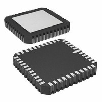
IC ADC 12BIT 10MSPS 44-CLCC
Manufacturer
Analog Devices Inc
Datasheet
1.AD872AJD.pdf
(20 pages)
Specifications of AD872AJE
Rohs Status
RoHS non-compliant
Number Of Bits
12
Sampling Rate (per Second)
10M
Data Interface
Parallel
Number Of Converters
7
Power Dissipation (max)
1.3W
Voltage Supply Source
Analog and Digital, Dual ±
Operating Temperature
0°C ~ 70°C
Mounting Type
Surface Mount
Package / Case
44-CLCC
Available stocks
Company
Part Number
Manufacturer
Quantity
Price


AD872A
SWITCHING SPECIFICATIONS
Parameter
Clock Period
CLOCK Pulsewidth High
CLOCK Pulsewidth Low
Clock Duty Cycle
Output Delay
Pipeline Delay (Latency)
Data Access Time (LCC Package Only)
Output Float Delay (LCC Package Only)
NOTES
1
2
Specifications subject to change without notice.
ABSOLUTE MAXIMUM RATINGS
Parameter
AV
AV
DV
DRV
DRGND
AGND
AV
Clock Input, OEN
Digital Outputs
V
REF IN
Junction Temperature
Storage Temperature
Lead Temperature (10 sec)
NOTES
1
2
Conversion rate is operational down to 10 kHz without degradation in specified performance.
See section on Three-State Outputs for timing diagrams and applications information.
Stresses above those listed under Absolute Maximum Ratings may cause permanent damage to the device. This is a stress rating only; functional operation of the device
at these or any other conditions above those indicated in the operational sections of this specification is not implied. Exposure to absolute maximum ratings for extended
periods may affect device reliability.
LCC package only.
INA
DD
SS
DD
DD
, V
DD
, DRV
INB
2
, REF IN
DD
1
2
2
2
BIT 2–12
MSB, OTR
CLOCK
VIN
N
t
1
CH
N
2
t
C
2
t
CL
(T
V
N+1
IN
MIN
N+1
With Respect to
AGND
AGND
DGND, DRGND
DV
DGND
DGND
DV
DGND
DGND
AGND
AGND
= 2.0 V, V
to T
DD
DD
Figure 1. Timing Diagram
MAX
with AV
OL
= 0.4 V and V
Symbol
t
t
t
t
t
t
C
CH
CL
OD
DD
HL
DD
–4–
= +5 V, DV
2
OH
DATA
= 2.4 V)
N
DD
Min
–0.5
–6.5
–0.5
–6.5
–0.3
–1.0
–6.5
–0.5
–0.5
–6.5
AV
–65
= +5 V, DRV
SS
DATA
N+1
J, S Grades
100
45
45
40
60
10
3
50
50
t
OD
DD
= +5 V, AV
Max
+6.5
+0.5
+6.5
+6.5
+0.3
+1.0
+6.5
DV
DV
+6.5
AV
+150
+150
+300
DD
DD
DD
SS
= –5 V; V
+ 0.5
+ 0.3
Units
ns min
ns min
ns min
% min (50% typ)
% max
ns min (20 ns typ)
Clock Cycles
ns typ (100 pF Load)
ns typ (10 pF Load)
IL
= 0.8 V,
Units
Volts
Volts
Volts
Volts
Volts
Volts
Volts
Volts
Volts
Volts
Volts
C
C
C
REV. A
Related parts for AD872AJE
Image
Part Number
Description
Manufacturer
Datasheet
Request
R

Part Number:
Description:
±1.7g Dual-Axis IMEMS Accelerometer Evaluation Board
Manufacturer:
Analog Devices Inc
Datasheet:

Part Number:
Description:
Inertial Sensor Evaluation System
Manufacturer:
Analog Devices Inc
Datasheet:
Part Number:
Description:
Manufacturer:
Analog Devices Inc
Datasheet:
Part Number:
Description:
Manufacturer:
Analog Devices Inc
Datasheet:
Part Number:
Description:
Manufacturer:
Analog Devices Inc
Datasheet:
Part Number:
Description:
Manufacturer:
Analog Devices Inc
Datasheet:
Part Number:
Description:
Manufacturer:
Analog Devices Inc
Datasheet:
Part Number:
Description:
Manufacturer:
Analog Devices Inc
Datasheet:
Part Number:
Description:
Manufacturer:
Analog Devices Inc
Datasheet:
Part Number:
Description:
Manufacturer:
Analog Devices Inc
Datasheet:
Part Number:
Description:
Manufacturer:
Analog Devices Inc
Datasheet:
Part Number:
Description:
Manufacturer:
Analog Devices Inc
Datasheet:
Part Number:
Description:
Manufacturer:
Analog Devices Inc
Datasheet: