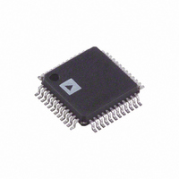
AD7664AST Analog Devices Inc, AD7664AST Datasheet - Page 15

AD7664AST
Manufacturer Part Number
AD7664AST
Description
IC ADC 16BIT UNIPOLAR 48-LQFP
Manufacturer
Analog Devices Inc
Series
PulSAR®r
Datasheet
1.AD7664ASTZ.pdf
(24 pages)
Specifications of AD7664AST
Rohs Status
RoHS non-compliant
Number Of Bits
16
Sampling Rate (per Second)
570k
Data Interface
Serial, Parallel
Number Of Converters
1
Power Dissipation (max)
115mW
Voltage Supply Source
Analog and Digital
Operating Temperature
-40°C ~ 85°C
Mounting Type
Surface Mount
Package / Case
48-LQFP
For Use With
EVAL-AD7664CBZ - BOARD EVALUATION FOR AD7664
Available stocks
Company
Part Number
Manufacturer
Quantity
Price
Company:
Part Number:
AD7664AST
Manufacturer:
ADI
Quantity:
329
Company:
Part Number:
AD7664ASTZ
Manufacturer:
AD
Quantity:
672
Company:
Part Number:
AD7664ASTZ
Manufacturer:
Analog Devices Inc
Quantity:
10 000
Part Number:
AD7664ASTZ
Manufacturer:
ADI/亚德诺
Quantity:
20 000
Company:
Part Number:
AD7664ASTZRL
Manufacturer:
Analog Devices Inc
Quantity:
10 000
CONVERSION CONTROL
Figure 11 shows the detailed timing diagrams of the conversion
process. The AD7664 is controlled by the signal CNVST, which
initiates conversion. Once initiated, it cannot be restarted or
aborted, even by the power-down input PD, until the conver-
sion is complete. The CNVST signal operates independently of
CS and RD signals.
In Impulse Mode, conversions can be automatically initiated. If
CNVST is held LOW when BUSY is LOW, the AD7664 controls
the acquisition phase and then automatically initiates a new
conversion. By keeping CNVST LOW, the AD7664 keeps the
conversion process running by itself. It should be noted that the
analog input has to be settled when BUSY goes LOW. Also, at
power-up, CNVST should be brought LOW once to initiate the
conversion process. In this mode, the AD7664 could sometimes
run slightly faster then the guaranteed limits in the Impulse
Mode of 444 kSPS. This feature does not exist in Warp or
Normal Modes.
Although CNVST is a digital signal, it should be designed with
special care with fast, clean edges, and levels with minimum
overshoot and undershoot or ringing.
It is a good thing to shield the CNVST trace with ground and
also to add a low value serial resistor (i.e., 50 Ω) termination
close to the output of the component that drives this line.
For applications where the SNR is critical, the CNVST signal
should have a very low jitter. This may be achieved by using a
dedicated oscillator for CNVST generation or, at least, to clock
it with a high frequency, low jitter clock as shown in Figure 5.
REV. E
CNVST
MODE
BUSY
DATABUS
RESET
CNVST
BUSY
ACQUIRE
t
t
3
5
Figure 11. Basic Conversion Timing
Figure 12. RESET Timing
t
CONVERT
1
t
7
t
4
t
9
t
t
2
6
ACQUIRE
t
8
t
8
CONVERT
–15–
DIGITAL INTERFACE
The AD7664 has a versatile digital interface; it can be interfaced
with the host system by using either a serial or parallel interface.
The serial interface is multiplexed on the parallel databus. The
AD7664 digital interface also accommodates both 3 V or 5 V logic
by simply connecting the OVDD supply pin of the AD7664 to
the host system interface digital supply. Finally, by using the
OB/2C input pin, either twos complement or straight binary
coding can be used.
The two signals CS and RD control the interface. CS and RD
have a similar effect, because they are OR’d together internally.
When at least one of these signals is HIGH, the interface out-
puts are in high impedance. Usually, CS allows the selection of
each AD7664 in multicircuit applications and is held LOW in a
single AD7664 design. RD is generally used to enable the con-
version result on the databus.
PARALLEL INTERFACE
The AD7664 is configured to use the parallel interface when
the SER/PAR is held LOW. The data can be read either after
each conversion, which is during the next acquisition phase,
or during the following conversion as shown, respectively, in
Figures 14 and 15. When the data is read during the conversion,
however, it is recommended that it be read-only during the first
half of the conversion phase. This avoids any potential feed-
through between voltage transients on the digital interface and
the most critical analog conversion circuitry.
DATA BUS
DATABUS
CS = RD = 0
CNVST
Figure 13. Master Parallel Data Timing for Reading
(Continuous Read)
Figure 14. Slave Parallel Data Timing for Reading
(Read after Convert)
BUSY
BUSY
CS
RD
t
t
3
12
PREVIOUS CONVERSION DATA
CONVERSION
t
1
CURRENT
t
13
t
10
t
4
AD7664
t
11
NEW DATA


