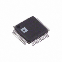
AD7664AST Analog Devices Inc, AD7664AST Datasheet - Page 14

AD7664AST
Manufacturer Part Number
AD7664AST
Description
IC ADC 16BIT UNIPOLAR 48-LQFP
Manufacturer
Analog Devices Inc
Series
PulSAR®r
Datasheet
1.AD7664ASTZ.pdf
(24 pages)
Specifications of AD7664AST
Rohs Status
RoHS non-compliant
Number Of Bits
16
Sampling Rate (per Second)
570k
Data Interface
Serial, Parallel
Number Of Converters
1
Power Dissipation (max)
115mW
Voltage Supply Source
Analog and Digital
Operating Temperature
-40°C ~ 85°C
Mounting Type
Surface Mount
Package / Case
48-LQFP
For Use With
EVAL-AD7664CBZ - BOARD EVALUATION FOR AD7664
Available stocks
Company
Part Number
Manufacturer
Quantity
Price
Company:
Part Number:
AD7664AST
Manufacturer:
ADI
Quantity:
329
Company:
Part Number:
AD7664ASTZ
Manufacturer:
AD
Quantity:
672
Company:
Part Number:
AD7664ASTZ
Manufacturer:
Analog Devices Inc
Quantity:
10 000
Part Number:
AD7664ASTZ
Manufacturer:
ADI/亚德诺
Quantity:
20 000
Company:
Part Number:
AD7664ASTZRL
Manufacturer:
Analog Devices Inc
Quantity:
10 000
AD7664
The AD8021 meets these requirements and is usually appropri-
ate for almost all applications. The AD8021 needs an external
compensation capacitor of 10 pF. This capacitor should have
good linearity as an NPO ceramic or mica type.
The AD8022 could also be used where a dual version is needed
and a gain of 1 is used.
The AD829 is another alternative where high frequency (above
100 kHz) performance is not required. In a gain of 1, it requires
an 82 pF compensation capacitor.
The AD8610 is another option where low bias current is needed
in low frequency applications.
Voltage Reference Input
The AD7664 uses an external 2.5 V voltage reference.
The voltage reference input REF of the AD7664 has a dynamic
input impedance; it should, therefore, be driven by a low imped-
ance source with an efficient decoupling between REF and
REFGND inputs. This decoupling depends on the choice of the
voltage reference, but usually consists of a 1 µF ceramic capacitor
and a low ESR tantalum capacitor connected to the REF and
REFGND inputs with minimum parasitic inductance. 47 µF is an
appropriate value for the tantalum capacitor when used with one
of the recommended reference voltages:
For applications using multiple AD7664s, it is more effective to
buffer the reference voltage with a low noise, very stable op amp
like the AD8031.
Care should also be taken with the reference temperature coeffi-
cient of the voltage reference that directly affects the full-scale
accuracy, if this parameter matters. For instance, a ± 15 ppm/°C
tempco of the reference changes the full scale by ± 1 LSB/°C.
V
AVDD – 1.85 V. The benefit here is the increased SNR obtained
as a result of this increase. Since the input range is defined in
terms of V
a 0 V to 3 V input range with an AVDD above 4.85 V. The
theoretical improvement as a result of this increase in reference is
1.58 dB (20 log [3/2.5]). Due to the theoretical quantization noise,
however, the observed improvement is approximately 1 dB. The
AD780 can be selected with a 3 V reference voltage.
Power Supply
The AD7664 uses three sets of power supply pins: an analog 5 V
supply AVDD, a digital 5 V core supply DVDD, and a digital
input/output interface supply OVDD. The OVDD supply allows
direct interface with any logic working between 2.7 V and 5.25 V.
To reduce the number of supplies needed, the digital core
REF
• The driver needs to have a THD performance suitable to that
• The low noise, low temperature drift ADR421 and AD780
• The low power ADR291 voltage reference
• The low cost AD1582 voltage reference
For instance, in a driver like the AD8021, with an equivalent
input noise of 2 nV/√Hz and configured as a buffer, thus with a
noise gain of 1, the SNR degrades by 0.58 dB.
of the AD7664. TPC 12 gives the THD versus frequency
that the driver should preferably exceed.
voltage references
, as mentioned in the specification table, could be increased to
REF
, this would essentially increase the range to make it
–14–
(DVDD) can be supplied through a simple RC filter from the
analog supply as shown in Figure 5. The AD7664 is independent
of power supply sequencing and thus free from supply voltage
induced latch-up. Additionally, it is very insensitive to power supply
variations over a wide frequency range, as shown in Figure 9.
POWER DISSIPATION VERSUS THROUGHPUT
Operating currents are very low during the acquisition phase, which
allows significant power savings when the conversion rate is
reduced, as shown in Figure 10. This power saving depends on the
mode used. In Impulse Mode, the AD7664 automatically reduces
its power consumption at the end of each conversion phase. This
feature makes the AD7664 ideal for very low power battery-
operated applications. It should be noted that the digital interface
remains active even during the acquisition phase. To reduce the
operating digital supply currents even further, the digital inputs
need to be driven close to the power supply rails (i.e., DVDD or
DGND for all inputs except EXT/INT, INVSYNC, INVSCLK,
RDC/SDIN, and OVDD or OGND for these last four inputs).
100k
Figure 10. Power Dissipation vs. Sample Rate
–50
–55
–60
–65
–70
–75
–80
10k
100
0.1
1k
10
1
1
0.1
Figure 9. PSRR vs. Frequency
1
10
INPUT FREQUENCY – kHz
SAMPLING RATE – SPS
10
WARP/NORMAL
100
IMPULSE
1k
100
10k
100k
1000
1M
REV. E


