AD679SD Analog Devices Inc, AD679SD Datasheet - Page 9
AD679SD
Manufacturer Part Number
AD679SD
Description
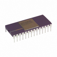
IC ADC 14BIT SAMPLING 28-CDIP
Manufacturer
Analog Devices Inc
Datasheet
1.AD679JNZ.pdf
(16 pages)
Specifications of AD679SD
Rohs Status
RoHS non-compliant
Number Of Bits
14
Sampling Rate (per Second)
128k
Data Interface
Parallel
Number Of Converters
2
Power Dissipation (max)
745mw
Voltage Supply Source
Analog and Digital, Dual ±
Operating Temperature
-55°C ~ 125°C
Mounting Type
Through Hole
Package / Case
28-CDIP (0.600", 15.24mm)
Available stocks
Company
Part Number
Manufacturer
Quantity
Price


REV. D
CONVERSION CONTROL
In synchronous mode (SYNC = HIGH), both chip select (CS)
and start convert (SC) must be brought LOW to start a conver-
sion. CS should be LOW t
asynchronous mode (SYNC = LOW), a conversion is started by
bringing SC low, regardless of the state of CS.
Before a conversion is started, end-of-convert (EOC) is HIGH
and the sample-and-hold is in track mode. After a conversion is
started, the sample-and-hold goes into hold mode and EOC
goes LOW, signifying that a conversion is in progress. During
the conversion, the sample-and-hold will go back into track
mode and start acquiring the next sample.
In track mode, the sample-and-hold will settle to 0.003%
(14 bits) in 1.5 µs maximum. The acquisition time does not
affect the throughput rate as the AD679 goes back into track
mode more than 2 µs before the next conversion. In multichan-
nel systems, the input channel can be switched as soon as EOC
goes LOW.
Bringing OE LOW t
register contents available on the output data bits (DB7–DB0).
A period of time, t
before the next SC instruction is issued.
If SC is held LOW, conversion accuracy may deteriorate. For
this reason, SC should not be held low in an attempt to operate
in a continuously converting mode.
Synchronous
Mode
Asynchronous
Mode
1 = HIGH voltage level.
0 = LOW voltage level.
X = Don’t care.
f = HIGH to LOW transition. Must stay low for t = t
Unipolar Coding
(Straight Binary)
V
0.00000 V
5.00000 V
9.99939 V
*Code center.
IN
Table II. 14-Bit Mode Coding Format (1 LSB = 0.61 mV)
*
Table I. Start Conversion Truth Table
Output Code
000 . . . 0
100 . . . 0
111 . . . 1
SYNC
CD
1
1
1
1
0
0
0
OE
, is required after OE is brought HIGH
after CS goes LOW makes the output
Inputs
CS
SC
X
X
X
1
0
f
0
before SC is brought LOW. In
SC
Bipolar Coding
(Twos Complement)
V
0.00000
+2.50000
+4.99939
–5.00000
–0.00061
X
1
f
0
0
f
0
IN
* (V)
Status
No Conversion
Start Conversion
Start Conversion
(Not Recommended)
Continuous Conversion
(Not Recommended)
No Conversion
Start Conversion
Continuous Conversion
(Not Recommended)
CP
.
Output Code
100 . . . 0
111 . . . 1
000 . . . 0
010 . . . 0
011 . . . 1
–9–
END-OF-CONVERT
In asynchronous mode, end-of-convert (EOC) is an open-drain
output (requiring a minimum 3 kΩ pull-up resistor) enabled by
end-of-convert enable (EOCEN). In synchronous mode, EOC
is a three-state output that is enabled by EOCEN and CS. See
Table III. Access (t
not apply in asynchronous mode where they are a function of
the time constant formed by the external load capacitance and
the pull-up resistor.
OUTPUT ENABLE OPERATION
The data bits (DB7–DB0) are three-state outputs that are enabled
by chip select (CS) and output enable (OE). CS should be
LOW t
When EOC goes HIGH, the conversion is completed and the
output data may be read. The output is read in two steps as a
16-bit word, with the high byte read first, followed by the low
byte. High byte enable (HBE) controls the output sequence.
The 14-bit result is left justified within the 16-bit field.
In unipolar mode (BIPOFF tied to AGND), the output coding
is straight binary. In bipolar mode (BIPOFF tied to REF
output coding is twos complement binary.
POWER-UP
The AD679 typically requires 10 µs after power-up to reset
internal logic.
Synchronous
Mode
Asynchronous
Mode*
1 = HIGH voltage level.
0 = LOW voltage level.
X = Don’t care.
*EOC requires a pull-up resistor in asynchronous mode.
Unipolar or
Bipolar
1 = HIGH voltage level.
0 = LOW voltage level.
X = Don’t care.
U = Logical OR.
Data coding is binary for unipolar mode and twos complement binary for
bipolar mode.
OE
before OE is brought LOW.
Table III. Conversion Status Truth Table
Table IV. Output Enable Truth Table
SYNC CS EOCEN EOC
1
1
1
1
0
0
0
HBE
X
0
1
BA
Inputs
) and float (t
X
X
X
X
0
0
1
a = MSB.
n = LSB.
Inputs
(CS U OE)
1
0
0
X
0
0
1
0
0
1
FD
Output
0
1
High Z
High Z
0
High Z
High Z
) timing specifications do
a b c d e f g h
i j k l m n 0 0
DB7 . . . DB0
← High Z →
Status
Converting
Not Converting
Either
Either
Converting
Not Converting
Either
Outputs
AD679
OUT
),
Related parts for AD679SD
Image
Part Number
Description
Manufacturer
Datasheet
Request
R

Part Number:
Description:
±1.7g Dual-Axis IMEMS Accelerometer Evaluation Board
Manufacturer:
Analog Devices Inc
Datasheet:

Part Number:
Description:
Inertial Sensor Evaluation System
Manufacturer:
Analog Devices Inc
Datasheet:
Part Number:
Description:
Manufacturer:
Analog Devices Inc
Datasheet:
Part Number:
Description:
Manufacturer:
Analog Devices Inc
Datasheet:
Part Number:
Description:
Manufacturer:
Analog Devices Inc
Datasheet:
Part Number:
Description:
Manufacturer:
Analog Devices Inc
Datasheet:
Part Number:
Description:
Manufacturer:
Analog Devices Inc
Datasheet:
Part Number:
Description:
Manufacturer:
Analog Devices Inc
Datasheet:
Part Number:
Description:
Manufacturer:
Analog Devices Inc
Datasheet:
Part Number:
Description:
Manufacturer:
Analog Devices Inc
Datasheet:
Part Number:
Description:
Manufacturer:
Analog Devices Inc
Datasheet:
Part Number:
Description:
Manufacturer:
Analog Devices Inc
Datasheet:
Part Number:
Description:
Manufacturer:
Analog Devices Inc
Datasheet: