AD679SD Analog Devices Inc, AD679SD Datasheet - Page 6
AD679SD
Manufacturer Part Number
AD679SD
Description
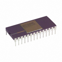
IC ADC 14BIT SAMPLING 28-CDIP
Manufacturer
Analog Devices Inc
Datasheet
1.AD679JNZ.pdf
(16 pages)
Specifications of AD679SD
Rohs Status
RoHS non-compliant
Number Of Bits
14
Sampling Rate (per Second)
128k
Data Interface
Parallel
Number Of Converters
2
Power Dissipation (max)
745mw
Voltage Supply Source
Analog and Digital, Dual ±
Operating Temperature
-55°C ~ 125°C
Mounting Type
Through Hole
Package / Case
28-CDIP (0.600", 15.24mm)
Available stocks
Company
Part Number
Manufacturer
Quantity
Price


AD679
Mnemonic Pin No.
AGND
AIN
BIPOFF
CS
DGND
DB7–DB0
EOC
EOCEN
HBE
OE
with
REF
REF
SC
SYNC
V
V
V
—
—
Type: AI = Analog Input. AO = Analog Output. DI = Digital Input (TTL and 5 V CMOS compatible). DO = Digital Output (TTL and 5 V CMOS compatible).
All DO pins are three-state drivers. P = Power. U = Unused.
CC
EE
DD
IN
OUT
28-Lead
DIP
7
6
10
4
12, 14
26–19
27
1
15
2
9
8
3
13
11
5
28
16
17–18
REF
EOCEN
BIPOFF
AGND
DGND
DGND
REF
SYNC
V
AIN
OUT
V
OE
SC
CS
EE
CC
IN
DIP Package
10
11
12
13
14
40, 39, 37, 36,
44-Lead
JLCC
Pin No.
11
10
15
6
23
35, 34, 33, 31
42
1
25
3
14
12
5
21
17
8
43
2, 4, 7, 9, 13,
16, 18, 19, 20,
22, 24, 26, 27,
28, 29, 30, 32,
38, 41, 44
1
2
3
4
5
6
7
8
9
(Not to Scale)
TOP VIEW
AD679
28
27
26
25
24
23
22
21
20
19
18
17
16
15
V
EOC
DB7
DB6
DB5
DB4
DB3
DB2
DB1
DB0
DGND
DGND
DGND
HBE
DD
Type
P
AI
AI
DI
P
DO
DO
DI
DI
DI
AI
AO
DI
DI
P
P
P
U
U
PIN FUNCTION DESCRIPTIONS
Name and Function
Analog Ground. This is the ground return for AIN only.
Analog Signal Input.
Bipolar Offset. Connect to AGND for +10 V input unipolar mode and straight
binary output coding. Connect to REF
twos complement binary output coding.
Chip Select. Active LOW.
Digital Ground.
Data Bits. These pins provide all 14 bits in two bytes (8 + 6 bits). Active HIGH.
End-of-Convert. EOC goes LOW when a conversion starts and goes HIGH
when the conversion finishes. In asynchronous mode, EOC is an open-drain
output and requires an external 3 kΩ pull-up resistor. See EOCEN and SYNC
pins for information on EOC gating.
End-of-Convert Enable. Enables EOC pin. Active LOW.
High Byte Enable. If LOW, output contains high byte. If HIGH, output
contains low byte (corresponding to the most recently read high byte).
Output Enable. A down-going transition on OE enables DB7 to DB0. Gated
CS. Active LOW.
Reference Input. 5 V input gives 10 V full-scale range.
5 V Reference Output. Tied to REF
Start Convert. Active LOW. See SYNC pin for gating.
SYNC Control. If tied to V
by CS. If tied to DGND (asynchronous mode), SC and EOCEN are indepen-
dent of CS, and EOC is an open-drain output. EOC requires an external 3 kΩ
pull-up resistor in asynchronous mode.
12 V Analog Power.
–12 V Analog Power.
5 V Digital Power.
Tie to DGND.
These pins are unused and should be connected to DGND or V
PIN CONFIGURATIONS
–6–
REF
BIPOFF
DD
NC = NO CONNECT
AGND
REF
V
V
OUT
AIN
NC
NC
NC
NC
CC
EE
(synchronous mode), SC and EOCEN are gated
IN
10
11
12
13
14
15
16
17
7 7
8
9
IN
18 19 20 21 22 23 24 25 26 27 28
6
for normal operation.
OUT
5
JLCC Package
4
for
3
(Not to Scale)
TOP VIEW
IDENTIFIER
AD679
2
PIN 1
5 V input bipolar mode and
1 44 43 42 41 40
DD
36
29
39
38
37
35
34
33
32
31
30
.
DB6
NC
DB5
DB4
DB3
DB2
DB1
NC
DB0
NC
NC
REV. D
Related parts for AD679SD
Image
Part Number
Description
Manufacturer
Datasheet
Request
R

Part Number:
Description:
±1.7g Dual-Axis IMEMS Accelerometer Evaluation Board
Manufacturer:
Analog Devices Inc
Datasheet:

Part Number:
Description:
Inertial Sensor Evaluation System
Manufacturer:
Analog Devices Inc
Datasheet:
Part Number:
Description:
Manufacturer:
Analog Devices Inc
Datasheet:
Part Number:
Description:
Manufacturer:
Analog Devices Inc
Datasheet:
Part Number:
Description:
Manufacturer:
Analog Devices Inc
Datasheet:
Part Number:
Description:
Manufacturer:
Analog Devices Inc
Datasheet:
Part Number:
Description:
Manufacturer:
Analog Devices Inc
Datasheet:
Part Number:
Description:
Manufacturer:
Analog Devices Inc
Datasheet:
Part Number:
Description:
Manufacturer:
Analog Devices Inc
Datasheet:
Part Number:
Description:
Manufacturer:
Analog Devices Inc
Datasheet:
Part Number:
Description:
Manufacturer:
Analog Devices Inc
Datasheet:
Part Number:
Description:
Manufacturer:
Analog Devices Inc
Datasheet:
Part Number:
Description:
Manufacturer:
Analog Devices Inc
Datasheet: