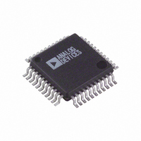
AD9260AS Analog Devices Inc, AD9260AS Datasheet - Page 27

AD9260AS
Manufacturer Part Number
AD9260AS
Description
IC ADC CMOS 16BIT OVRSAMP 44MQFP
Manufacturer
Analog Devices Inc
Datasheet
1.AD9260ASZRL.pdf
(44 pages)
Specifications of AD9260AS
Rohs Status
RoHS non-compliant
Number Of Bits
16
Sampling Rate (per Second)
20M
Data Interface
Parallel
Number Of Converters
1
Power Dissipation (max)
585mW
Voltage Supply Source
Analog and Digital
Operating Temperature
-40°C ~ 85°C
Mounting Type
Surface Mount
Package / Case
44-MQFP, 44-PQFP
Available stocks
Company
Part Number
Manufacturer
Quantity
Price
Company:
Part Number:
AD9260ASZ
Manufacturer:
ADI
Quantity:
100
Company:
Part Number:
AD9260ASZ
Manufacturer:
Analog Devices Inc
Quantity:
10 000
Part Number:
AD9260ASZ
Manufacturer:
ADI/亚德诺
Quantity:
20 000
Company:
Part Number:
AD9260ASZRL
Manufacturer:
Analog Devices Inc
Quantity:
10 000
beyond the input signals passband by adding a shunt capacitor,
C
essentially establish a low-pass filter which reduces the noise
gain to one beyond the filter’s f
bandlimiting the input signal to f
established by this filter can also be used as the real pole of an
antialiasing filter. Since the noise contribution of two op amps
from the same product family are typically equal but
uncorrelated, the total output-referred noise of each op amp
will add root-sum square leading to a further 3 dB degradation
in the circuit’s noise performance. Further out-of-band noise
reduction can be realized with the addition of single-ended and
differential capacitors, C
The distortion and noise performance of the two op amps
within the signal path are critical in achieving optimum
performance in the AD9260. Low noise op amps capable of
providing greater than 85 dB THD at 1 MHz while swinging
over a 1 V to 3 V range are a rare commodity, yet these parts are
the only ones that should be considered. The AD9632 op amp
was found to provide superb distortion performance in this
circuit due to its ability to maintain excellent distortion
performance over a wide bandwidth while swinging over a 1 V
to 3 V range. Since the AD9632 is gain-of-two or greater stable,
the use of the noise reduction shunt capacitors discussed above
was prohibited, thus degrading its noise performance slightly
F
, across the feedback resistor of each op amp. This will
VIN
Figure 64. DC-Coupled Differential Driver with Level-Shifting
R
R
R
R
C
C
R
R
R
R
F
F
S
V
100pF
V
100pF
CML
and C
CML
50Ω
C
C
-VIN
50Ω
C
C
-VIN
–3
D
dB while simultaneously
.
–3
dB. Note that the pole
C
100pF
0.1µF
D
AD817
1.0µF
50Ω
50Ω
AD9260
VINA
VINB
CML
Rev. C | Page 27 of 44
(1 dB–2 dB) when compared to the OPA642. Note that the
majority of the AD9260 test and characterization data presented
in this data sheet was taken using the AD9632 op amp in this
dc-coupled driver circuit. This driver circuit is also provided on
the AD9260 evaluation board since the AD8138 was unreleased
at that time.
The outputs of each op amp are ac coupled via a small series
resistor and capacitor (i.e., 50 Ω and 0.1 µF) to the respective
inputs of the AD9260. Similar to the dc coupled driver, further
out-of-band noise reduction can be realized with the addition of
100 pF single-ended and differential capacitors, C
lower cutoff frequency of this ac-coupled circuit is determined
by R
CML, of the AD9260 for proper biasing of the inputs. Although
the OPA642 was found to provide the lowest overall noise and
distortion performance (88.8 dB and 96 dB THD @ 100 kHz),
the AD8055, or dual AD8056, suffered only a 0.5 dB to 1.5 dB
degradation in overall performance. It is worth noting that
given the high level of performance attainable by the AD9260,
special consideration must be given to both the quality of the
test equipment and test set-up in its evaluation.
Common-Mode Level
The CML pin is an internal analog bias point used internally by
the AD9260. This pin must be decoupled to analog ground with
at least a 0.1 µF capacitor as shown in Figure 65. The dc level of
CML is approximately AVDD/2.5. This voltage should be
buffered if it is to be used for any external biasing.
Note: the common-mode voltage of the input signal applied to
the AD9260 need not be at the exact same level as CML. While
this level is recommended for optimal performance, the
AD9260 is tolerant of a range of input common-mode voltages
around AVDD/2.5.
C
and C
C
in which R
0.1µF
Figure 65. CML Decoupling
C
is tied to the common-mode level pin,
CML
AD9260
S
and C
AD9260
D
. The


