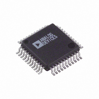
AD9260AS Analog Devices Inc, AD9260AS Datasheet - Page 23

AD9260AS
Manufacturer Part Number
AD9260AS
Description
IC ADC CMOS 16BIT OVRSAMP 44MQFP
Manufacturer
Analog Devices Inc
Datasheet
1.AD9260ASZRL.pdf
(44 pages)
Specifications of AD9260AS
Rohs Status
RoHS non-compliant
Number Of Bits
16
Sampling Rate (per Second)
20M
Data Interface
Parallel
Number Of Converters
1
Power Dissipation (max)
585mW
Voltage Supply Source
Analog and Digital
Operating Temperature
-40°C ~ 85°C
Mounting Type
Surface Mount
Package / Case
44-MQFP, 44-PQFP
Available stocks
Company
Part Number
Manufacturer
Quantity
Price
Company:
Part Number:
AD9260ASZ
Manufacturer:
ADI
Quantity:
100
Company:
Part Number:
AD9260ASZ
Manufacturer:
Analog Devices Inc
Quantity:
10 000
Part Number:
AD9260ASZ
Manufacturer:
ADI/亚德诺
Quantity:
20 000
Company:
Part Number:
AD9260ASZRL
Manufacturer:
Analog Devices Inc
Quantity:
10 000
THEORY OF OPERATION
The AD9260 utilizes a new analog-to-digital converter
architecture to combine sigma-delta techniques with a high
speed, pipelined A/D converter. This topology allows the
AD9260 to offer the high dynamic range associated with sigma-
delta converters while maintaining very wide input signal
bandwidth (1.25 MHz) at a very modest 8 oversampling ratio.
Figure 59 provides a block diagram of the AD9260. The
differential analog input is fed into a second order, multibit
sigma-delta modulator. This modulator features a 5-bit flash
quantizer and 5-bit feedback. In addition, a 12-bit pipelined
A/D quantizes the input to the 5-bit flash to greater accuracy. A
special digital modulation loop combines the output of the 12-
bit pipelined A/D with the delayed output of the 5-bit flash to
produce the equivalent response of a second order loop with a
12-bit quantizer and 12-bit feedback. The combination of a
second order loop and multibit feedback provides inherent
stability: the AD9260 is not prone to the idle tones or full-scale
idiosyncrasies sometimes associated with higher order single bit
sigma-delta modulators.
The output of this 12-bit modulator is fed into the digital
decimation filter. The voltage level on the MODE pin
establishes the configuration for the digital filter. The user may
bring the data out undecimated (at the clock rate), or at a
decimation factor of 2×, 4×, or a full 8×. The spectra for these
four cases are shown in Figure 11, Figure 12, Figure 13, and
Figure 14, all for a 100 kHz full-scale input and 20 MHz clock.
The spectra of the undecimated output clearly shows the second
order shaping characteristic of the quantization noise as it rises
at frequencies above 1.25 MHz.
The on-chip decimation filter provides excellent stopband
rejection to suppress any stray input signal between 1.25 MHz
and 18.75 MHz, substantially easing the requirements on any
Rev. C | Page 23 of 44
antialiasing filter for the analog input path. The decimation
filters are integrated with symmetric FIR filter structures,
providing a linear phase response and excellent passband
flatness. The digital output driver register of the AD9260
features both READ and CHIP SELECT pins to allow easy
interfacing. The digital supply of the AD9260 is designed to
operate over a 2.7 V to 5.25 V supply range, though 3 V supplies
are recommended to minimize digital noise on the board. A
DATA AVAILABLE pin allows the user to easily synchronize to
the converter’s decimated output data rate. OUT-OF-RANGE
(OTR) indication is given for an overflow in the pipelined A/D
converter or digital filters. A RESETB function is provided to
synchronize the converter’s decimated data and clear any
overflow condition in the analog integrators.
An on-chip reference and reference buffer are included on the
AD9260. The reference can be configured in either a 2.5 V
mode (providing a 4 V p-p differential input full scale), a 1 V
mode (providing a 1.6 V p-p differential input full scale), or
programmed with an external resistor divider to provide any
voltage level between 1 V and 2.5 V. However, optimum noise
and distortion performance for the AD9260 can only be achieved
with a 2.5 V reference, as shown in Figure 52.
For users who want to operate the part at reduced clock
frequencies, the bias current of the AD9260 is designed to be
scalable. This scaling is accomplished through use of the proper
external resistor tied to the BIAS pin: the power can be reduced
roughly proportionately to clock frequency by as much as 75%
(for clock rates of 5 MHz). Refer to Figure 47 to Figure 49 and
Figure 53 to Figure 57 for characterization curves showing
performance tradeoffs.
AD9260


