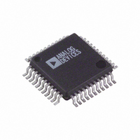
AD9260AS Analog Devices Inc, AD9260AS Datasheet - Page 13

AD9260AS
Manufacturer Part Number
AD9260AS
Description
IC ADC CMOS 16BIT OVRSAMP 44MQFP
Manufacturer
Analog Devices Inc
Datasheet
1.AD9260ASZRL.pdf
(44 pages)
Specifications of AD9260AS
Rohs Status
RoHS non-compliant
Number Of Bits
16
Sampling Rate (per Second)
20M
Data Interface
Parallel
Number Of Converters
1
Power Dissipation (max)
585mW
Voltage Supply Source
Analog and Digital
Operating Temperature
-40°C ~ 85°C
Mounting Type
Surface Mount
Package / Case
44-MQFP, 44-PQFP
Available stocks
Company
Part Number
Manufacturer
Quantity
Price
Company:
Part Number:
AD9260ASZ
Manufacturer:
ADI
Quantity:
100
Company:
Part Number:
AD9260ASZ
Manufacturer:
Analog Devices Inc
Quantity:
10 000
Part Number:
AD9260ASZ
Manufacturer:
ADI/亚德诺
Quantity:
20 000
Company:
Part Number:
AD9260ASZRL
Manufacturer:
Analog Devices Inc
Quantity:
10 000
PIN CONFIGURATION AND FUNCTION DESCRIPTIONS
Table 11. Pin Function Descriptions
Pin No.
1
2, 29, 38
3
4, 28, 44
5
6
7
8
9
10–23
24
25
26
27
30
31
32
33
34
35
36
37
39
40, 43
41
42
Mnemonic
DVSS
AVSS
DVDD
AVDD
DRVSS
DRVDD
CLK
READ
BIT16
BIT15–BIT2
BIT1
OTR
DAV
CS
RESET
SENSE
VREF
REFCOM
MODE
BIAS
CAPB
CAPT
CML
NC
VINA
VINB
(LSB) BIT16
Description
Digital Ground.
Analog Ground.
+3 V to +5 V Digital Supply.
+5 V Analog Supply.
Digital Output Driver Ground.
+3 V to +5 V Digital Output Driver Supply.
Clock Input.
Part of DSP Interface—Pull Low to Disable Output Bits.
Least Significant Data Bit (LSB).
Data Output Bit.
Most Significant Data Bit (MSB).
Out of Range—Set When Converter or Filter Overflows.
Data Available.
Chip Select (CS): Active LOW.
RESET : Active LOW.
Reference Amplifier SENSE: Selects REF Level.
Input Span Select Reference I/O.
Reference Common.
Mode Select—Selects Decimation Mode.
Power Bias.
Noise Reduction Pin—Decouples Reference Level.
Noise Reduction Pin—Decouples Reference Level.
Common-Mode Level (AVDD/2.5).
No Connect (Ground for Shielding Purposes).
Analog Input Pin (+).
Analog Input Pin (–).
DRVDD
DRVSS
READ
DVDD
AVDD
BIT15
BIT14
DVSS
AVSS
CLK
NC = NO CONNECT
10
11
1
2
3
4
5
6
7
8
9
44
12
PIN 1
IDENTIFIER
43
13
Figure 10. Pin Configuration
Rev. C | Page 13 of 44
42
14
15
41
(Not to Scale)
40
16
AD9260
TOP VIEW
39
17
38
18
37
19
36
20
35
21
34
22
33
32
30
29
28
27
26
25
24
23
31
REFCOM
VREF
SENSE
RESET
AVSS
AVDD
CS
DAV
OTR
BIT1 (MSB)
BIT2
AD9260


