MAX1301BEUP+ Maxim Integrated Products, MAX1301BEUP+ Datasheet - Page 4
MAX1301BEUP+
Manufacturer Part Number
MAX1301BEUP+
Description
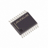
IC ADC 16BIT SER 4CH LP 20TSSOP
Manufacturer
Maxim Integrated Products
Datasheet
1.MAX1301BEUPT.pdf
(32 pages)
Specifications of MAX1301BEUP+
Number Of Bits
16
Sampling Rate (per Second)
115k
Data Interface
MICROWIRE™, QSPI™, Serial, SPI™
Number Of Converters
1
Power Dissipation (max)
105.5mW
Voltage Supply Source
Analog and Digital
Operating Temperature
-40°C ~ 85°C
Mounting Type
Surface Mount
Package / Case
20-TSSOP
Lead Free Status / RoHS Status
Lead free / RoHS Compliant


8- and 4-Channel, ±3 x V
Serial 16-Bit ADCs
ELECTRICAL CHARACTERISTICS (continued)
(AV
external clock mode, V
(±3 x V
4
INTERNAL REFERENCE (Bypass REFCAP with 0.1μF to AGND1 and REF with 1.0μF to AGND1)
Reference Output Voltage
Reference Temperature
Coefficient
Reference Short-Circuit Current
Reference Load Regulation
EXTERNAL REFERENCE (REFCAP = AV
Reference Input Voltage Range
REFCAP Buffer Disable
Threshold
Reference Input Current
Reference Input Resistance
DIGITAL INPUTS (DIN, SCLK, CS)
Input High Voltage
Input Low Voltage
Input Hysteresis
Input Leakage Current
Input Capacitance
DIGITAL OUTPUTS (DOUT, SSTRB)
Output Low Voltage
Output High Voltage
DOUT Tri-State Leakage Current
POWER REQUIREMENTS (AV
Analog Supply Voltage
Digital Supply Voltage
DD1
_______________________________________________________________________________________
REF
= AV
), C
PARAMETER
DD2
DOUT
= DV
= 50pF, C
DD
REF
= DV
= 4.096V (external reference operation), REFCAP = AV
SSTRB
DDO
DD1
= 50pF, T
= 5V, AGND1 = DGND = DGNDO = AGND2 = AGND3 = 0, f
and AGND1, AV
SYMBOL
I
AV
TC
V
V
DV
REFSC
R
V
V
I
I
V
RCTH
V
HYST
C
DDO
V
REF
V
I
REF
REF
REF
IN
OH
OL
DD1
REF
IH
IN
IL
DD
DD
A
)
= -40°C to +85°C, unless otherwise noted. Typical values are at T
REF shorted to AGND1
REF shorted to AV
I
(Note 5)
V
external acquisition mode, internal clock
mode, or partial power-down mode
V
External clock mode, external
acquisition mode, internal clock mode,
or partial power-down mode
Full power-down mode
V
DV
DV
I
REF
SOURCE
REF
REF
IN
DDO
DDO
= DV
= 0 to DV
DD2
= 0 to 0.5mA
= +4.096V, external clock mode,
= +4.096V, full power-down mode
= 4.75V, I
= 2.7V, I
DDO
and AGND2, DV
= 0.5mA
DDO
CONDITIONS
SINK
SINK
REF
DD
= 5mA
= 10mA
DD
and DGND, DV
Multirange Inputs,
DD1
, maximum single-ended bipolar input range
DDO
DV
DV
AV
4.056
3.800
0.7 x
- 0.4
- 0.4
4.75
4.75
MIN
-10
-10
20
DDO
DDO
DD1
and DGNDO)
CLK
= 3.5MHz (50% duty cycle),
4.096
TYP
±0.1
±30
0.1
0.2
10
90
45
40
10
-1
A
= +25°C.)
DV
AV
4.136
4.136
MAX
0.3 x
- 0.1
5.25
5.25
±10
+10
+10
200
0.4
0.4
10
DDO
DD1
ppm/°C
UNITS
mA
M
mV
μA
k
μA
μA
pF
V
V
V
V
V
V
V
V
V
V
Related parts for MAX1301BEUP+
Image
Part Number
Description
Manufacturer
Datasheet
Request
R

Part Number:
Description:
(MAX1300 / MAX1301) Serial 16-Bit ADCs
Manufacturer:
Maxim Integrated Products

Part Number:
Description:
MAX CLIP
Manufacturer:
Aavid Thermalloy
Datasheet:
Part Number:
Description:
MAX7528KCWPMaxim Integrated Products [CMOS Dual 8-Bit Buffered Multiplying DACs]
Manufacturer:
Maxim Integrated Products
Datasheet:
Part Number:
Description:
Single +5V, fully integrated, 1.25Gbps laser diode driver.
Manufacturer:
Maxim Integrated Products
Datasheet:
Part Number:
Description:
Single +5V, fully integrated, 155Mbps laser diode driver.
Manufacturer:
Maxim Integrated Products
Datasheet:
Part Number:
Description:
VRD11/VRD10, K8 Rev F 2/3/4-Phase PWM Controllers with Integrated Dual MOSFET Drivers
Manufacturer:
Maxim Integrated Products
Datasheet:
Part Number:
Description:
Highly Integrated Level 2 SMBus Battery Chargers
Manufacturer:
Maxim Integrated Products
Datasheet:
Part Number:
Description:
Current Monitor and Accumulator with Integrated Sense Resistor; ; Temperature Range: -40°C to +85°C
Manufacturer:
Maxim Integrated Products
Part Number:
Description:
TSSOP 14/A°/RS-485 Transceivers with Integrated 100O/120O Termination Resis
Manufacturer:
Maxim Integrated Products
Part Number:
Description:
TSSOP 14/A°/RS-485 Transceivers with Integrated 100O/120O Termination Resis
Manufacturer:
Maxim Integrated Products
Part Number:
Description:
QFN 16/A°/AC-DC and DC-DC Peak-Current-Mode Converters with Integrated Step
Manufacturer:
Maxim Integrated Products
Part Number:
Description:
TDFN/A/65V, 1A, 600KHZ, SYNCHRONOUS STEP-DOWN REGULATOR WITH INTEGRATED SWI
Manufacturer:
Maxim Integrated Products
Part Number:
Description:
Integrated Temperature Controller f
Manufacturer:
Maxim Integrated Products
Part Number:
Description:
SOT23-6/I°/45MHz to 650MHz, Integrated IF VCOs with Differential Output
Manufacturer:
Maxim Integrated Products
Part Number:
Description:
SOT23-6/I°/45MHz to 650MHz, Integrated IF VCOs with Differential Output
Manufacturer:
Maxim Integrated Products