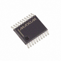
MAX1301BEUP+ Maxim Integrated Products, MAX1301BEUP+ Datasheet - Page 22

MAX1301BEUP+
Manufacturer Part Number
MAX1301BEUP+
Description
IC ADC 16BIT SER 4CH LP 20TSSOP
Manufacturer
Maxim Integrated Products
Datasheet
1.MAX1301BEUPT.pdf
(32 pages)
Specifications of MAX1301BEUP+
Number Of Bits
16
Sampling Rate (per Second)
115k
Data Interface
MICROWIRE™, QSPI™, Serial, SPI™
Number Of Converters
1
Power Dissipation (max)
105.5mW
Voltage Supply Source
Analog and Digital
Operating Temperature
-40°C ~ 85°C
Mounting Type
Surface Mount
Package / Case
20-TSSOP
Lead Free Status / RoHS Status
Lead free / RoHS Compliant
The MAX1300/MAX1301 contain one byte-wide mode-
control register. The timing diagram of Figure 15 shows
how to use the mode-control byte, and the mode-con-
trol byte format is shown in Table 7. The mode-control
byte is used to select the conversion method and to
control the power modes of the MAX1300/MAX1301.
8- and 4-Channel, ±3 x V
Serial 16-Bit ADCs
Figure 12. Ideal Bipolar Transfer Function, Single-Ended or
Differential Input
Figure 14. Ideal Unipolar Transfer Function, Single-Ended
Input, 0 to +FSR
22
______________________________________________________________________________________
FFFD
FFFD
FFFF
FFFE
8001
8000
7FFF
0003
0002
0001
0000
FFFF
FFFE
8001
8000
7FFF
0003
0002
0001
0000
(AGND1)
-32,768 -32,766
0
1
2
3
INPUT VOLTAGE (LSB [DECIMAL])
INPUT VOLTAGE (LSB [DECIMAL])
AGND1 (DIF/SGL = 0)
OV (DIF/SGL = 1)
-1
32,768
FSR
FSR
0
+1
1 LSB =
1 LSB =
65,536 x 4.096V
65,536 x 4.096V
FSR x V
FSR x V
Mode Control
+32,765 +32,767
65,533 65,535
REF
REF
REF
The conversion method is selected using the mode-con-
trol byte (see the Mode Control section), and the conver-
sion is initiated using a conversion-start command (Table
3, and Figures 2, 3, and 4).The MAX1300/MAX1301 con-
vert analog signals to digital data using one of three
methods:
•
•
•
Figure 13. Ideal Unipolar Transfer Function, Single-Ended
Input, -FSR to 0
External Clock Mode, Mode 0 (Figure 2)
• Highest maximum throughput (see the Electrical
• User controls the sample instant
• CS remains low during the conversion
• User supplies SCLK throughout the ADC con-
External Acquisition Mode, Mode 1 (Figure 3)
• Lowest maximum throughput (see the Electrical
• User controls the sample instant
• User supplies two bytes of SCLK, then drives
• After SSTRB transitions high, the user supplies
Internal Clock Mode, Mode 2 (Figure 4)
• High maximum throughput (see the Electrical
Characteristics table)
version and reads data at DOUT
Characteristics table)
CS high to relieve processor load while the ADC
converts
two bytes of SCLK and reads data at DOUT
Characteristics table)
FFFD
FFFF
FFFE
8001
8000
7FFF
0003
0002
0001
0000
Multirange Inputs,
0
1
2
3
Selecting the Conversion Method
INPUT VOLTAGE (LSB [DECIMAL])
32,768
FSR
1 LSB =
65,536 x 4.096V
FSR x V
65,533 65,535
REF
(AGND1)


