ADADC80-12 Analog Devices Inc, ADADC80-12 Datasheet - Page 3
ADADC80-12
Manufacturer Part Number
ADADC80-12
Description
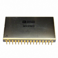
IC ADC 12-BIT INTEGRATED 32-CDIP
Manufacturer
Analog Devices Inc
Datasheet
1.ADADC80-12.pdf
(16 pages)
Specifications of ADADC80-12
Data Interface
Parallel
Rohs Status
RoHS non-compliant
Number Of Bits
12
Sampling Rate (per Second)
40k
Number Of Converters
1
Power Dissipation (max)
800mW
Voltage Supply Source
Analog and Digital, Dual ±
Operating Temperature
-25°C ~ 85°C
Mounting Type
Through Hole
Package / Case
32-CDIP (0.900", 22.86mm)
Resolution (bits)
12bit
Input Channel Type
Single Ended
Supply Current
70mA
Digital Ic Case Style
DIP
No. Of Pins
32
Operating Temperature Range
-25°C To +85°C
Number Of Elements
1
Resolution
12Bit
Architecture
SAR
Input Polarity
Unipolar/Bipolar
Input Type
Voltage
Rated Input Volt
5/10/±2.5/±5/±10V
Differential Input
No
Power Supply Requirement
Dual
Single Supply Voltage (typ)
Not RequiredV
Single Supply Voltage (min)
Not RequiredV
Single Supply Voltage (max)
Not RequiredV
Dual Supply Voltage (typ)
±15/5V
Dual Supply Voltage (min)
±14/4.75V
Dual Supply Voltage (max)
±16/5.25V
Differential Linearity Error
±0.5LSB(Typ)
Integral Nonlinearity Error
±0.012%FSR
Operating Temp Range
-25C to 85C
Operating Temperature Classification
Commercial
Mounting
Through Hole
Pin Count
32
Package Type
SBCDIP
Input Signal Type
Single-Ended
Lead Free Status / Rohs Status
Not Compliant
Available stocks
Company
Part Number
Manufacturer
Quantity
Price

Part Number:
ADADC80-12
Manufacturer:
AD
Quantity:
20 000


SPECIFICATIONS
Typical @ 25°C, ±15 V, and +5 V, unless otherwise noted.
Table 1.
Parameter
RESOLUTION
ANALOG INPUTS
DIGITAL INPUTS
TRANSFER CHARACTERISTICS ERROR
DRIFT
CONVERSION SPEED
DIGITAL OUTPUTS (ALL CODES COMPLEMENTARY)
Voltage Ranges
Impedance (Direct Input)
Positive Pulse During Conversion (CONVERT
START)
Logic Loading
External Clock (EXTERNAL CLOCK IN)
Gain Error
Offset
Linearity Error
Inherent Quantization Error
Differential Linearity Error
No Missing Codes Temperature Range
Power Supply Sensitivity
Specification Temperature Range
Gain
Offset
Linearity
Monotonicity
Parallel, BIT 1 (MSB) to BIT 12 (LSB)
Status (STATUS)
Internal Clock (CLOCK OUT)
Bipolar
Unipolar
0 to +5, ±2.5 V
0 to +10, ±5 V
±10 V
Bipolar
Unipolar
±15 V
+5 V
Bipolar
Unipolar
Output Codes
Output Drive
Status Output Drive
Clock Output Drive
Frequency
Bipolar
Unipolar
2
2
8
1
4
7
6
5
Min
100
−25
−25
17
Rev. E | Page 3 of 16
Typ
12
±2.5 or ±5 or ±10
0 to +5 or 0 to +10
2.5
5
10
1
1
±0.1
±0.1
±0.05
±½
±½
±0.0030
±0.0015
±3
Guaranteed
22
COB, CTC
CSB
2
Logic 1 during conversion
2
2
575
Max
±0.012
+85
+85
±30
±15
±3
25
Unit
Bits
V
V
kΩ
kΩ
kΩ
ns
TTL load
TTL load
% of FSR
% of FSR
% of FSR
% of FSR
LSB
LSB
°C
% of FSR/% V
% of FSR/% V
°C
ppm/°C
ppm of FSR/°C
ppm of FSR/°C
ppm of FSR/°C
μs
TTL loads
TTL loads
TTL loads
kHz
ADADC80
3
S
S
Related parts for ADADC80-12
Image
Part Number
Description
Manufacturer
Datasheet
Request
R

Part Number:
Description:
IC ADC 12BIT INTEGRATED 32-CDIP
Manufacturer:
Analog Devices Inc
Datasheet:

Part Number:
Description:
±1.7g Dual-Axis IMEMS Accelerometer Evaluation Board
Manufacturer:
Analog Devices Inc
Datasheet:

Part Number:
Description:
Inertial Sensor Evaluation System
Manufacturer:
Analog Devices Inc
Datasheet:
Part Number:
Description:
Manufacturer:
Analog Devices Inc
Datasheet:
Part Number:
Description:
Manufacturer:
Analog Devices Inc
Datasheet:
Part Number:
Description:
Manufacturer:
Analog Devices Inc
Datasheet:
Part Number:
Description:
Manufacturer:
Analog Devices Inc
Datasheet:
Part Number:
Description:
Manufacturer:
Analog Devices Inc
Datasheet:
Part Number:
Description:
Manufacturer:
Analog Devices Inc
Datasheet:
Part Number:
Description:
Manufacturer:
Analog Devices Inc
Datasheet:
Part Number:
Description:
Manufacturer:
Analog Devices Inc
Datasheet:
Part Number:
Description:
Manufacturer:
Analog Devices Inc
Datasheet:
Part Number:
Description:
Manufacturer:
Analog Devices Inc
Datasheet: