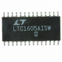
LTC1605AISW#PBF Linear Technology, LTC1605AISW#PBF Datasheet - Page 8

LTC1605AISW#PBF
Manufacturer Part Number
LTC1605AISW#PBF
Description
IC A/D CONV 16BIT SAMPLNG 28SOIC
Manufacturer
Linear Technology
Datasheet
1.LTC1605INPBF.pdf
(16 pages)
Specifications of LTC1605AISW#PBF
Number Of Bits
16
Sampling Rate (per Second)
100k
Data Interface
Parallel
Number Of Converters
1
Power Dissipation (max)
80mW
Voltage Supply Source
Analog and Digital
Operating Temperature
-40°C ~ 85°C
Mounting Type
Surface Mount
Package / Case
28-SOIC (0.300", 7.50mm Width)
Number Of Elements
1
Resolution
16Bit
Architecture
SAR
Sample Rate
100KSPS
Input Polarity
Bipolar
Input Type
Voltage
Rated Input Volt
±10V
Differential Input
No
Power Supply Requirement
Analog and Digital
Single Supply Voltage (typ)
5V
Single Supply Voltage (min)
4.75V
Single Supply Voltage (max)
5.25V
Dual Supply Voltage (typ)
Not RequiredV
Dual Supply Voltage (min)
Not RequiredV
Dual Supply Voltage (max)
Not RequiredV
Power Dissipation
80mW
Differential Linearity Error
1LSB
Integral Nonlinearity Error
±2LSB
Operating Temp Range
-40C to 85C
Operating Temperature Classification
Industrial
Mounting
Surface Mount
Pin Count
28
Package Type
SOIC W
Input Signal Type
Single-Ended
Lead Free Status / RoHS Status
Lead free / RoHS Compliant
Available stocks
Company
Part Number
Manufacturer
Quantity
Price
LTC1605
APPLICATIONS
Conversion Details
The LTC1605 uses a successive approximation algorithm
and an internal sample-and-hold circuit to convert an
analog signal to a 16-bit or two byte parallel output. The
ADC is complete with a precision reference and an internal
clock. The control logic provides easy interface to micro-
processors and DSPs. (Please refer to the Digital Interface
section for the data format.)
Conversion start is controlled by the CS and R/C inputs. At
the start of conversion the successive approximation
register (SAR) is reset. Once a conversion cycle has begun
it cannot be restarted.
During the conversion, the internal 16-bit capacitive DAC
output is sequenced by the SAR from the most significant
bit (MSB) to the least significant bit (LSB). Referring to
Figure 1, V
the sample-and-hold capacitor during the acquire phase
and the comparator offset is nulled by the autozero switches.
In this acquire phase, a minimum delay of 2µs will provide
enough time for the sample-and-hold capacitor to acquire
the analog signal. During the convert phase, the autozero
switches open, putting the comparator into the compare
mode. The input switch switches C
injecting the analog input charge onto the summing junc-
tion. This input charge is successively compared with the
binary-weighted charges supplied by the capacitive DAC.
Bit decisions are made by the high speed comparator. At
the end of a conversion, the DAC output balances the V
input charge. The SAR contents (a 16-bit data word) that
represents the V
8
V
IN
R
IN1
R
Figure 1. LTC1605 Simplified Equivalent Circuit
IN2
IN
is connected through the resistor divider to
SAMPLE
HOLD
IN
are loaded into the 16-bit output latches.
U
C
SAMPLE
C
V
DAC
DAC
INFORMATION
U
DAC
W
SAMPLE
SAMPLE
–
+
COMPARATOR
SI
to ground,
U
16-BIT
LATCH
1605 • F01
R
S
A
IN
Driving the Analog Inputs
The nominal input range for the LTC1605 is ±10V or
(±4 • V
The input impedance is typically 20kΩ, therefore, it should
be driven with a low impedance source. Wideband noise
coupling into the input can be minimized by placing a
1000pF capacitor at the input as shown in Figure 2. An
NPO-type capacitor gives the lowest distortion. Place the
capacitor as close to the device input pin as possible. If an
amplifier is to be used to drive the input, care should be
taken to select an amplifier with adequate accuracy, linear-
ity and noise for the application. The following list is a
summary of the op amps that are suitable for driving the
LTC1605. More detailed information is available in the
Linear Technology data books and LinearView
LT1007 - Low noise precision amplifier. 2.7mA supply
current ±5V to ±15V supplies. Gain bandwidth product
8MHz. DC applications.
LT1097 - Low cost, low power precision amplifier. 300µA
supply current. ±5V to ±15V supplies. Gain bandwidth
product 0.7MHz. DC applications.
LT1227 - 140MHz video current feedback amplifier. 10mA
supply current. ±5V to ±15V supplies. Low noise and low
distortion.
LT1360 - 37MHz voltage feedback amplifier. 3.8mA sup-
ply current. ±5V to ±15V supplies. Good AC/DC specs.
LT1363 - 50MHz voltage feedback amplifier. 6.3mA sup-
ply current. Good AC/DC specs.
LT1364/LT1365 - Dual and quad 50MHz voltage feedback
amplifiers. 6.3mA supply current per amplifier. Good AC/
DC specs.
LinearView is a trademark of Linear Technology Corporation
REF
) and the input is overvoltage protected to ±25V.
A
IN
Figure 2. Analog Input Filtering
200Ω
1000pF
33.2k
V
CAP
1605 • F02
IN
TM
CD-ROM.
1605fc


