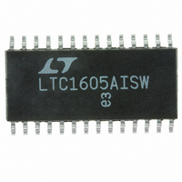
LTC1605AISW#PBF Linear Technology, LTC1605AISW#PBF Datasheet - Page 7

LTC1605AISW#PBF
Manufacturer Part Number
LTC1605AISW#PBF
Description
IC A/D CONV 16BIT SAMPLNG 28SOIC
Manufacturer
Linear Technology
Datasheet
1.LTC1605INPBF.pdf
(16 pages)
Specifications of LTC1605AISW#PBF
Number Of Bits
16
Sampling Rate (per Second)
100k
Data Interface
Parallel
Number Of Converters
1
Power Dissipation (max)
80mW
Voltage Supply Source
Analog and Digital
Operating Temperature
-40°C ~ 85°C
Mounting Type
Surface Mount
Package / Case
28-SOIC (0.300", 7.50mm Width)
Number Of Elements
1
Resolution
16Bit
Architecture
SAR
Sample Rate
100KSPS
Input Polarity
Bipolar
Input Type
Voltage
Rated Input Volt
±10V
Differential Input
No
Power Supply Requirement
Analog and Digital
Single Supply Voltage (typ)
5V
Single Supply Voltage (min)
4.75V
Single Supply Voltage (max)
5.25V
Dual Supply Voltage (typ)
Not RequiredV
Dual Supply Voltage (min)
Not RequiredV
Dual Supply Voltage (max)
Not RequiredV
Power Dissipation
80mW
Differential Linearity Error
1LSB
Integral Nonlinearity Error
±2LSB
Operating Temp Range
-40C to 85C
Operating Temperature Classification
Industrial
Mounting
Surface Mount
Pin Count
28
Package Type
SOIC W
Input Signal Type
Single-Ended
Lead Free Status / RoHS Status
Lead free / RoHS Compliant
Available stocks
Company
Part Number
Manufacturer
Quantity
Price
on Pin 15 and bit 8 is output on Pin 22. Bit 7 is output on
Pin 6 and the LSB is output on Pin 13.
R/C (Pin 24): Read/Convert Input. With CS low, a falling
edge on R/C puts the internal sample-and-hold into the
hold state and starts a conversion. With CS low, a rising
edge on R/C enables the output data bits.
CS (Pin 25): Chip Select. Internally OR’d with R/C. With
R/C low, a falling edge on CS will initiate a conversion.
With R/C high, a falling edge on CS will enable the output
data.
FUNCTIONAL BLOCK DIAGRA
TEST CIRCUITS
PIN
U
U
DBN
FUNCTIONS
A. HI-Z TO V
AGND1
AGND2
(2.5V)
DGND
CAP
REF
V
IN
U
1k
U
OH
Load Circuit for Access Timing
AND V
20k
4k
OL
U
REF BUF
TO V
2.5V REF
C
OH
L
10k
INTERNAL
CLOCK
4k
B. HI-Z TO V
DBN
OL
AND V
5V
1k
16-BIT CAPACITIVE DAC
SUCCESSIVE APPROXIMATION
W
CS
C
OH
LTC1605 • TC01
L
TO V
C
C
SAMPLE
SAMPLE
CONTROL LOGIC
OL
REGISTER
R/C
BUSY (Pin 26): Output Shows Converter Status. It is low
when a conversion is in progress. Data valid on the rising
edge of BUSY. CS or R/C must be high when BUSY rises
or another conversion will start without time for signal
acquisition.
V
a 0.1µF ceramic and a 10µF tantalum capacitor.
V
27.
ANA
DIG
DBN
BYTE
(Pin 28): 5V Digital Supply. Connect directly to Pin
(Pin 27): 5V Analog Supply. Bypass to ground with
BUSY
A. V
1k
Load Circuit for Output Float Delay
ZEROING SWITCHES
16
OH
TO HI-Z
+
–
COMP
OUTPUT LATCHES
50pF
DBN
LTC1605 • BD
B. V
LTC1605
OL
•
•
•
5V
TO HI-Z
D15
D0
V
V
1k
LTC1605 • TC02
ANA
DIG
50pF
1605fc
7


