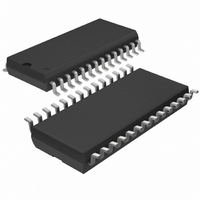
LTC1419AISW Linear Technology, LTC1419AISW Datasheet

LTC1419AISW
Specifications of LTC1419AISW
Available stocks
Related parts for LTC1419AISW
LTC1419AISW Summary of contents
Page 1
... There is no pipeline delay in the conversion results. A separate convert start input and data ready signal (BUSY) ease connections to FIFOs, DSPs and microprocessors. , LT, LTC and LTM are registered trademarks of Linear Technology Corporation. All other trademarks are the property of their respective owners. Protected by U.S. Patents including 5581252. ...
Page 2
... CS = High Between Conversions During Conversions – 2.5V < (– < 2. ORDER TOP VIEW PART NUMBER LTC1419ACG BUSY LTC1419ACSW LTC1419AIG 6 23 CONVST LTC1419AISW SHDN LTC1419CG LTC1419CSW LTC1419IG LTC1419ISW PACKAGE 28-LEAD PLASTIC SO = 125°C, θ = 95°C/W ( 125°C, θ = 130°C/W (SW) JA http://www.linear.com/leadfree/ ...
Page 3
ACCURACY otherwise specifications are 25°C. (Note 5) A SYMBOL PARAMETER S/( Signal-to-(Noise + Distortion) Ratio THD Total Harmonic Distortion SFDR Spurious Free Dynamic Range IMD Intermodulation Distortion Full-Power Bandwidth Full-Linear ...
Page 4
LTC1419 W U POWER REQUIRE E TS otherwise specifications are 25°C. (Note 5) A SYMBOL PARAMETER P Power Dissipation DIS Nap Mode Sleep Mode CHARACTERISTICS range, otherwise specifications are at T SYMBOL ...
Page 5
W U TYPICAL PERFORMANCE CHARACTERISTICS S/( Input Frequency and Amplitude 0dB –20dB –60dB 10k 100k 1M 2M ...
Page 6
LTC1419 CTIO S (Pin 1): ±2.5V Positive Analog Input (Pin 2): ±2.5V Negative Analog Input. – (Pin 3): 2.5V Reference Output. Bypass to AGND REF with 1µF. REFCOMP (Pin ...
Page 7
TEST CIRCUITS Load Circuits for Access Timing DBN DBN (A) Hi APPLICATIONS INFORMATION CONVERSION DETAILS The LTC1419 uses a successive approximation algorithm and an internal sample-and-hold circuit to convert an analog signal ...
Page 8
LTC1419 U U APPLICATIONS INFORMATION frequencies outside the fundamental. Figure 2 shows a typical LTC1419 FFT plot SAMPLE f = 99.804687kHz IN – 20 SFDR = 98dB THD = –93.3dB – 40 – 60 – 80 –100 –120 ...
Page 9
U U APPLICATIONS INFORMATION 0 –10 –20 –30 –40 –50 –60 –70 –80 THD –90 –100 3RD – 110 1k 10k 100k INPUT FREQUENCY (Hz) Figure 4. Distortion vs Input Frequency Intermodulation Distortion If the ADC input signal consists of ...
Page 10
... DC accuracy and settling time are most critical. The following list is a summary of the op amps that are suitable for driving the LTC1419. More detailed informa- tion is available in the Linear Technology databooks, the TM LinearView CD-ROM and on our web site at www.linear- tech ...
Page 11
U U APPLICATIONS INFORMATION many applications. For example, Figure 7 shows a 1000pF capacitor from + A to ground and a 100Ω source resistor IN to limit the input bandwidth to 1.6MHz. The 1000pF capacitor also acts as a charge ...
Page 12
LTC1419 U U APPLICATIONS INFORMATION Differential Inputs The LTC1419 has a unique differential sample-and-hold circuit that allows rail-to-rail inputs. The ADC will always convert the difference – (– common mode voltage (see Figure 11a). The ...
Page 13
U U APPLICATIONS INFORMATION applied to the – A input. For zero offset error, apply IN – 152µV (i.e., – 0.5LSB and adjust the offset at the IN – A input until the output code flickers between ...
Page 14
LTC1419 U U APPLICATIONS INFORMATION 1419fb ...
Page 15
U U APPLICATIONS INFORMATION Figure 13b. Suggested Evaluation Circuit Board—Component Side Silkscreen Figure 13c. Suggested Evaluation Circuit Board—Component Side Layout W U LTC1419 1419fb 15 ...
Page 16
LTC1419 U U APPLICATIONS INFORMATION Figure 13d. Suggested Evaluation Circuit Board—Solder Side Layout DIGITAL INTERFACE The A/D converter is designed to interface with micropro- cessors as a memory mapped device. The CS and RD control inputs are common to all ...
Page 17
U U APPLICATIONS INFORMATION SHDN t 3 CONVST Figure 14b. SHDN to CONVST Wake-Up Timing Timing and Control Conversion start and data read operations are controlled by three digital inputs: CONVST, CS and RD. A logic “0” applied to the ...
Page 18
LTC1419 U U APPLICATIONS INFORMATION CONVST BUSY DATA (N – 1) DATA DB13 TO DB0 Figure 17. Mode 1b. CONVST Starts a Conversion. Data Outputs Always Enabled (CONVST = CONVST ...
Page 19
... FLASH SHALL NOT EXCEED 0.254mm (0.010") PER SIDE Information furnished by Linear Technology Corporation is believed to be accurate and reliable. However, no responsibility is assumed for its use. Linear Technology Corporation makes no represen- tation that the interconnection of its circuits as described herein will not infringe on existing patent rights. ...
Page 20
... S28 (WIDE) 1098 ≤ 800ksps, 80mW Dissipation SAMPLE LT 0506 REV B • PRINTED IN USA © LINEAR TECHNOLOGY CORPORATION 1997 1419fb ...


