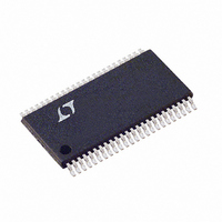
LTC1852IFW#PBF Linear Technology, LTC1852IFW#PBF Datasheet - Page 16

LTC1852IFW#PBF
Manufacturer Part Number
LTC1852IFW#PBF
Description
IC A/D CONV 8CH 10BIT 48-TSSOP
Manufacturer
Linear Technology
Datasheet
1.LTC1853CFWPBF.pdf
(24 pages)
Specifications of LTC1852IFW#PBF
Number Of Bits
10
Sampling Rate (per Second)
400k
Data Interface
Parallel
Number Of Converters
1
Power Dissipation (max)
15mW
Voltage Supply Source
Single Supply
Operating Temperature
-40°C ~ 85°C
Mounting Type
Surface Mount
Package / Case
48-TFSOP (0.240", 6.10mm Width)
Lead Free Status / RoHS Status
Lead free / RoHS Compliant
Available stocks
Company
Part Number
Manufacturer
Quantity
Price
LTC1852/LTC1853
APPLICATIONS INFORMATION
Power Shutdown
The LTC1852/LTC1853 provide two power shutdown
modes, Nap and Sleep, to save power during inactive
periods. The Nap mode reduces the power to 2.5mW and
leaves only the digital logic and reference powered up.
The wake-up time from Nap to active is 200ns. In Sleep
mode, all bias currents are shut down and only leakage
current remains—about 20μA. Wake-up time from sleep
mode is much slower since the reference circuit must
power-up and settle to 0.005% for full 12-bit accuracy
(0.02% for full 10-bit accuracy). Sleep mode wake-up time
is dependent on the value of the capacitor connected to
the REFCOMP (Pin 12). The wake-up time is 10ms with
the recommended 10μF capacitor.
Shutdown is controlled by Pin 47 (SHDN); the ADC is in
shutdown when it is low. The shutdown mode is selected
with Pin 46 (CS); low selects Nap (Figures 2 and 3).
Timing and Control
Conversion start and data read operations are controlled by
three digital inputs: CONVST, CS and RD (Figure 4). A logic
“0” applied to the CONVST pin will start a conversion after
16
Figure 4. CS to CONVST and RD Setup Timing
CONVST
RD
CS
Figure 5. Mode 1a CONVST Starts a Conversion. Data Outputs Always Enabled (CS = RD = 0)
t
CONVST
1
t
2
BUSY
DATA
t
6
DATA (N – 1)
18523 F04
t
5
t
CONV
t
7
the ADC has been selected (i.e., CS is low). Once initiated,
it cannot be restarted until the conversion is complete.
Converter status is indicated by the BUSY output. BUSY
is low during a conversion. If CONVST returns high at a
critical point during the conversion it can create small
errors. For the best results, ensure that CONVST returns
high either within 400ns after the start of the conversion
or after BUSY rises.
Figures 5 through 9 show several different modes
of operation. In modes 1a and 1b (Figures 5 and 6),
CS and RD are both tied low. The falling edge of
CONVST starts the conversion. The data outputs
are always enabled and data can be latched with the
BUSY rising edge. Mode 1a shows operation with a narrow
logic low CONVST pulse. Mode 1b shows a narrow logic
high CONVST pulse.
In mode 2 (Figure 7), CS is tied low. The falling edge of
CONVST signal again starts the conversion. Data out-
puts are in three-state until read by the MPU with the
RD signal. Mode 2 can be used for operation with a shared
MPU databus.
In slow memory and ROM modes (Figures 8 and 9),CS is
tied low and CONVST and RD are tied together. The MPU
starts the conversion and reads the output with the RD
signal. Conversions are started by the MPU or DSP (no
external sample clock).
In slow memory mode, the processor applies a logic low
to RD ( = CONVST), starting the conversion. BUSY goes
low, forcing the processor into a Wait state. The previous
conversion result appears on the data outputs. When
the conversion is complete, the new conversion results
t
8
DATA N
18523 F05
18523fa


