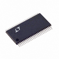
LTC1852IFW#PBF Linear Technology, LTC1852IFW#PBF Datasheet - Page 14

LTC1852IFW#PBF
Manufacturer Part Number
LTC1852IFW#PBF
Description
IC A/D CONV 8CH 10BIT 48-TSSOP
Manufacturer
Linear Technology
Datasheet
1.LTC1853CFWPBF.pdf
(24 pages)
Specifications of LTC1852IFW#PBF
Number Of Bits
10
Sampling Rate (per Second)
400k
Data Interface
Parallel
Number Of Converters
1
Power Dissipation (max)
15mW
Voltage Supply Source
Single Supply
Operating Temperature
-40°C ~ 85°C
Mounting Type
Surface Mount
Package / Case
48-TFSOP (0.240", 6.10mm Width)
Lead Free Status / RoHS Status
Lead free / RoHS Compliant
Available stocks
Company
Part Number
Manufacturer
Quantity
Price
LTC1852/LTC1853
APPLICATIONS INFORMATION
adjusted until the output code fl ickers between 1111 1111
1110 and 1111 1111 1111 for the LTC1853 and between
11 1111 1110 and 11 1111 1111 for the LTC1852.
For bipolar inputs, an input voltage of FS – 1.5LSBs should
be applied to the “+” input and the appropriate reference
adjusted until the output code fl ickers between 0111 1111
1110 and 0111 1111 1111 for the LTC1853 and between
01 1111 1110 and 01 1111 1111 for the LTC1852.
These adjustments as well as the factory trims affect all
channels. The channel-to-channel offset and gain error
matching are guaranteed by design to meet the specifi ca-
tions in the Converter Characteristics table.
OUTPUT DATA FORMAT
The LTC1852/LTC1853 have a 14 bit/16-bit parallel out-
put. The output word normally consists of a 10-bit/12-bit
conversion result data word and a 4-bit address (three
address bits A2
The output drivers are enabled when RD is low provided
the chip is selected (CS is low). All 14/16 data output pins
and BUSY are supplied by OV
interface to 3V or 5V digital logic.
The data format of the conversion result is automatically
selected and determined by the UNI/BIP input pin. If
the UNI/BIP pin is low indicating a unipolar input span
(0 – REFCOMP assuming PGA = 1), the format for the
data is straight binary with 1 LSB = FS/4096 (1mV for
REFCOMP = 4.096V). For the LTC1853 and 1LSB = FS/1024
(4mV for REFCOMP = 4.096V) for the LTC1852.
If the UNI/BIP pin is high indicating a bipolar input span
(± REFCOMP/2 for PGA = 1), the format for the data is two’s
complement binary with 1 LSB = [(+FS) – (–FS)]/4096
(1mV for REFCOMP = 4.096V). For the LTC1853 and 1LSB
= [(+FS) – (–FS)]/1024 (4mV for REFCOMP = 4.096V) for
the LTC1852.
In both cases, the code transitions occur midway be-
tween successive integer LSB values (i.e., –FS + 0.5LSB,
–FS + 1.5LSB, ... –1.5LSB, –0.5LSB, 0.5LSB, 1.5LSB, ...
FS – 1.5LSB, FS – 0.5LSB).
The three most signifi cant bits of the data word (D11, D10
and D9 for the LTC1853; D9, D8 and D7 for the LTC1852)
14
OUT
, A1
OUT
, A0
DD
OUT
and OGND to allow easy
and the DIFF
OUT
bit).
also function as output bits when reading the contents of
the programmable sequencer. During readback, a 7-bit
status word (S6-S0) containing the contents of the cur-
rent sequencer location is available when RD is low. The
individual bits of the status word are outlined in Figure 1.
During readback, the D8 to D0 pins (LTC1853) or D6 to
D0 pins (LTC1852) remain high impedance irrespective
of the state of RD.
1111...1111
1111...1110
1111...1101
1000...0001
1000...0000
0111...1111
0111...1110
0000...0010
0000...0001
0000...0000
0111...1111
0111...1110
0111...1101
0000...0001
0000...0000
1111...1111
1111...1110
1000...0010
1000...0001
1000...0000
DIFFERENTIAL BIT
SINGLE-ENDED/
Figure 1. Readback Status Word
S6
Unipolar Transfer Characteristic
(UNI/BIP = 0)
Bipolar Transfer Characteristic
(UNI/BIP = 1)
–FS
0
S5
A2
MUX ADDRESS
S4
A1
INPUT VOLTAGE (V)
INPUT VOLTAGE (V)
–1LBS 0 1LBS
BIPOLAR
S3
A0
ZERO
BIPOLAR BIT
UNIPOLAR/
S2
FS =
FS = V
PGA BIT
V
REFCOMP
S1
REFCOMP
SEQUENCE BIT
FS – 1LBS
2
FS – 1LBS
END OF
18523 F01A
18523 F01B
S0
18523 F01
18523fa


