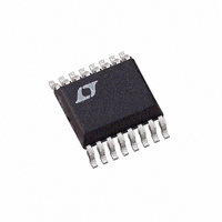
LTC2435-1IGN#TRPBF Linear Technology, LTC2435-1IGN#TRPBF Datasheet - Page 38

LTC2435-1IGN#TRPBF
Manufacturer Part Number
LTC2435-1IGN#TRPBF
Description
IC ADC DIFF I/REF 20BIT 16-SSOP
Manufacturer
Linear Technology
Datasheet
1.LTC2435-1CGN.pdf
(40 pages)
Specifications of LTC2435-1IGN#TRPBF
Number Of Bits
20
Sampling Rate (per Second)
13.75
Data Interface
MICROWIRE™, Serial, SPI™
Number Of Converters
2
Power Dissipation (max)
1mW
Voltage Supply Source
Single Supply
Operating Temperature
-40°C ~ 85°C
Mounting Type
Surface Mount
Package / Case
16-SSOP (0.150", 3.90mm Width)
Lead Free Status / RoHS Status
Lead free / RoHS Compliant
Available stocks
Company
Part Number
Manufacturer
Quantity
Price
LTC2435/LTC2435-1
APPLICATIO S I FOR ATIO
Correlated Double Sampling with the
LTC2435/LTC2435-1
The Typical Application on the back page of this data sheet
shows the LTC2435/LTC2435-1 in a correlated double
sampling circuit that achieves a noise floor of under
100nV. In this scheme, the polarity of the bridge is
alternated every other sample and the result is the average
of a pair of samples of opposite sign. This technique has
the benefit of canceling any fixed DC error components in
the bridge, amplifiers and the converter, as these will
alternate in polarity relative to the signal. Offset voltages
and currents, thermocouple voltages at junctions of dis-
similar metals and the lower frequency components of 1/f
noise are virtually eliminated.
The LTC2435/LTC2435-1 have the virtue of being able to
digitize an input voltage that is outside the range defined
by the reference, thereby providing a simple means to
implement a ratiometric example of correlated double
sampling.
This circuit uses a bipolar amplifier (LT1219—U1 and U2)
that has neither the lowest noise nor the highest gain. It
does, however, have an output stage that can effectively
suppress the conversion spikes from the LTC2435/
LTC2435-1. The LT1219 is a C-Load
that, by design, needs at least 0.1μF output capacitance to
remain stable. The 0.1μF ceramic capacitors at the out-
puts (C1 and C2) should be placed and routed to minimize
lead inductance or their effectiveness in preventing enve-
lope detection in the input stage will be reduced. Alterna-
tively, several smaller capacitors could be placed so that
lead inductance is further reduced. This is a consideration
because the frequency content of the conversion spikes
extends to 50MHz or more. The output impedance of
most op amps increases dramatically with frequency but
the effective output impedance of the LT1219 remains
38
U
U
W
TM
stable amplifier
U
low, determined by the ESR and inductance of the capaci-
tors above 10MHz. The conversion spikes that remain at
the output of other bipolar amplifiers pass through the
feedback network and often overdrive the input of the
amplifier, producing envelope detection. RFI may also be
present on the signal lines from the bridge; C3 and C4
provide RFI suppression at the signal input, as well as
suppressing transient voltages during bridge commuta-
tion.
The wideband noise density of the LT1219 is 33nV/√Hz,
seemingly much noisier than the lowest noise amplifiers.
However, in the region just below the 1/f corner that is not
well suppressed by the correlated double sampling, the
average noise density is similar to the noise density of
many low noise amplifiers. If the amplifier is rolled off
below about 1500Hz, the total noise bandwidth is deter-
mined by the converter’s Sinc
use of correlated double sampling involves averaging
even numbers of samples; hence, in this situation, two
samples would be averaged to give an input-referred
noise level of about 100nV
Level shift transistors Q4 and Q5 are included to allow
excitation voltages up to the maximum recommended for
the bridge. In the case shown, if a 10V supply is used, the
excitation voltage to the bridge is 8.5V and the outputs of
the bridge are above the supply rail of the ADC. U1 and U2
are also used to produce a level shift to bring the outputs
within the input range of the converter. This instrumenta-
tion amplifier topology does not require well-matched
resistors in order to produce good CMRR. However, the
use of R2 requires that R3 and R6 match well, as the
common mode gain is approximately –12dB. If the bridge
is composed of four equal 350Ω resistors, the differential
component associated with mismatch of R3 and R6 is
nearly constant with either polarity of excitation and, as
with offset, its contribution is canceled.
C-Load is a trademark of Linear Technology Corporation.
RMS
4
.
filter at about 12Hz. The
24351fb


