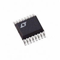
LTC2435-1IGN#TRPBF Linear Technology, LTC2435-1IGN#TRPBF Datasheet - Page 24

LTC2435-1IGN#TRPBF
Manufacturer Part Number
LTC2435-1IGN#TRPBF
Description
IC ADC DIFF I/REF 20BIT 16-SSOP
Manufacturer
Linear Technology
Datasheet
1.LTC2435-1CGN.pdf
(40 pages)
Specifications of LTC2435-1IGN#TRPBF
Number Of Bits
20
Sampling Rate (per Second)
13.75
Data Interface
MICROWIRE™, Serial, SPI™
Number Of Converters
2
Power Dissipation (max)
1mW
Voltage Supply Source
Single Supply
Operating Temperature
-40°C ~ 85°C
Mounting Type
Surface Mount
Package / Case
16-SSOP (0.150", 3.90mm Width)
Lead Free Status / RoHS Status
Lead free / RoHS Compliant
Available stocks
Company
Part Number
Manufacturer
Quantity
Price
LTC2435/LTC2435-1
APPLICATIO S I FOR ATIO
24
PRESERVING THE CONVERTER ACCURACY
The LTC2435/LTC2435-1 are designed to reduce as much
as possible conversion result sensitivity to device
decoupling, PCB layout, antialiasing circuits, line fre-
quency perturbations and so on. Nevertheless, in order to
preserve the extreme accuracy capability of this part,
some simple precautions are desirable.
Digital Signal Levels
The LTC2435/LTC2435-1 digital interface is easy to use.
Its digital inputs (F
operation) accept standard TTL/CMOS logic levels and the
internal hysteresis receivers can tolerate edge rates as slow
as 100μs. However, some considerations are required to
take advantage of the exceptional accuracy and low supply
current of this converter.
The digital output signals (SDO and SCK in Internal SCK
mode of operation) are less of a concern because they are
not generally active during conversion.
While a digital input signal is in the range 0.5V to
(V
current from the power supply. It should be noted that,
when any one of the digital input signals (F
in External SCK mode of operation) is within this range, the
LTC2435/LTC2435-1 power supply current may increase
even if the signal in question is at a valid logic level. For
micropower operation, it is recommended to drive all
digital input signals to full CMOS levels [V
V
During the conversion period, the undershoot and/or
overshoot of a fast digital signal connected to the LTC2435/
LTC2435-1 pins may severely disturb the analog to digital
conversion process. Undershoot and overshoot can oc-
cur because of the impedance mismatch at the converter
pin when the transition time of an external control signal
is less than twice the propagation delay from the driver to
LTC2435/LTC2435-1. For reference, on a regular FR-4
board, signal propagation velocity is approximately
183ps/inch for internal traces and 170ps/inch for surface
traces. Thus, a driver generating a control signal with a
minimum transition time of 1ns must be connected to the
OH
CC
> (V
– 0.5V), the CMOS input receiver draws additional
CC
– 0.4V)].
O
U
, CS and SCK in External SCK mode of
U
W
O
IL
, CS and SCK
< 0.4V and
U
converter pin through a trace shorter than 2.5 inches. This
problem becomes particularly difficult when shared con-
trol lines are used and multiple reflections may occur. The
solution is to carefully terminate all transmission lines
close to their characteristic impedance.
Parallel termination near the LTC2435/LTC2435-1 pins
will eliminate this problem but will increase the driver
power dissipation. A series resistor between 27Ω and 56Ω
placed near the driver or near the LTC2435/LTC2435-1
pins will also eliminate this problem without additional
power dissipation. The actual resistor value depends upon
the trace impedance and connection topology.
An alternate solution is to reduce the edge rate of the
control signals. It should be noted that using very slow
edges will increase the converter power supply current
during the transition time. The multiple ground pins used
in this package configuration, as well as the differential
input and reference architecture, reduce substantially the
converter’s sensitivity to ground currents.
Particular attention must be given to the connection of the
F
external conversion clock. This clock is active during the
conversion time and the normal mode rejection provided
by the internal digital filter is not very high at this fre-
quency. A normal mode signal of this frequency at the
converter reference terminals may result in DC gain and
INL errors. A normal mode signal of this frequency at the
converter input terminals may result in a DC offset error.
Such perturbations may occur due to asymmetric capaci-
tive coupling between the F
input and/or reference connection traces. An immediate
solution is to maintain maximum possible separation
between the F
nals. When the F
converter, substantial AC current is flowing in the loop
formed by the F
ground return path. Thus, perturbation signals may be
inductively coupled into the converter input and/or refer-
ence. In this situation, the user must reduce to a minimum
the loop area for the F
the differential input and reference connections.
O
signal when the LTC2435/LTC2435-1 are used with an
O
O
signal trace and the input/reference sig-
connection trace, the termination and the
O
signal is parallel terminated near the
O
signal as well as the loop area for
O
signal trace and the converter
24351fb


