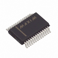
MAX1401EAI+ Maxim Integrated Products, MAX1401EAI+ Datasheet - Page 6

MAX1401EAI+
Manufacturer Part Number
MAX1401EAI+
Description
IC ADC 18BIT LP 28-SSOP
Manufacturer
Maxim Integrated Products
Datasheet
1.MAX1401EAI.pdf
(36 pages)
Specifications of MAX1401EAI+
Number Of Bits
18
Sampling Rate (per Second)
480
Data Interface
QSPI™, Serial, SPI™
Number Of Converters
1
Power Dissipation (max)
750µW
Voltage Supply Source
Analog and Digital
Operating Temperature
-40°C ~ 85°C
Mounting Type
Surface Mount
Package / Case
28-SSOP
Number Of Adc Inputs
5
Architecture
Delta-Sigma
Conversion Rate
4.8 KSPs
Resolution
18 bit
Input Type
Voltage
Interface Type
Serial
Voltage Reference
External
Supply Voltage (max)
3 V
Maximum Power Dissipation
21.45 mW
Maximum Operating Temperature
+ 85 C
Mounting Style
SMD/SMT
Input Signal Type
Pseudo-Differential, Differential
Minimum Operating Temperature
- 40 C
Lead Free Status / RoHS Status
Lead free / RoHS Compliant
+3V, 18-Bit, Low-Power, Multichannel,
Oversampling (Sigma-Delta) ADC
ELECTRICAL CHARACTERISTICS (continued)
(V+ = +2.7V to +3.6V, V
otherwise noted. Typical values are at T
6
Note 1: Contact factory for INL limits applicable with FS1 = 0 and MF1, MF0 = 1, 2, or 3.
Note 2: To achieve optimum INL performance with the MAX1401, ensure that the PCB layout carefully shields the MUXOUT and
Note 3: Nominal gain is 0.98. This ensures a full-scale input voltage may be applied to the part under all conditions without caus-
Note 4: Positive Full-Scale Error includes zero-scale errors (unipolar offset error or bipolar zero error) and applies to both unipolar
Note 5: Full-Scale Drift includes zero-scale drift (unipolar offset drift or bipolar zero drift) and applies to both unipolar and bipolar
Note 6: Gain Error does not include zero-scale errors. It is calculated as (full-scale error - unipolar offset error) for unipolar ranges
Note 7: Gain-Error Drift does not include unipolar offset drift or bipolar zero drift. It is effectively the drift of the part if zero-scale
Note 8: Use of the offset DAC does not imply that any input may be taken below AGND.
Note 9: Additional noise added by the offset DAC is dependent on the filter cutoff, gain, and DAC setting. No noise is added for a
Note 10: Guaranteed by design or characterization; not production tested.
Note 11: The input voltage must be within the Absolute Input Voltage Range specification.
Note 12: All AIN and REFIN pins have identical input structures. Leakage is production tested only for the AIN3, AIN4, AIN5,
Note 13: The dynamic load presented by the MAX1401 analog inputs for each gain setting is discussed in detail in the Switching
Note 14: The input voltage range for the analog inputs is with respect to the voltage on the negative input of its respective differen-
Note 15: V
POWER DISSIPATION (V+ = V
CLK = 0 for 1.024MHz, CLK = 1 for 2.4576MHz.)
Power Dissipation
Standby Power Dissipation
_______________________________________________________________________________________
PARAMETER
ADCIN pins from any digital noise source. The MAX1401’s INL is production tested with 150pF connected between
MUXOUT+ and MUXOUT- to minimize the effect of differential coupling from the CLKIN and CLKOUT pins.
ing saturation of the digital output data.
and bipolar input ranges. This error does not include the nominal gain of 0.98.
input ranges.
and as (full-scale error - bipolar zero error) for bipolar ranges. This error does not include the nominal gain of 0.98.
error is removed.
DAC code of 0000.
CALGAIN, and CALOFF inputs.
Network section. Values are provided for the maximum allowable external series resistance. Note that this value does not
include any additional capacitance added by the user to the MUXOUT_ or ADCIN_ pins.
tial or pseudo-differential pair. Table 5 shows which inputs form differential pairs.
REF
= V
REFIN+
DD
- V
= +2.7V to +3.6V, V
REFIN-
DD
.
SYMBOL
= +3.3V, digital inputs = 0 or V
PD
A
= +25°C.)
Normal mode,
MF1 = 0,
MF0 = 0
2X mode,
MF1 = 0,
MF0 = 1
4X mode,
MF1 = 1,
MF0 = 0
8X mode,
MF1 = 1,
MF0 = 1
(Note 20)
REFIN+
= +1.25V, REFIN- = AGND, f
CONDITIONS
1.024MHz
2.4576MHz
1.024MHz
2.4576MHz
1.024MHz
2.4576MHz
1.024MHz
2.4576MHz
DD
, external CLKIN, burn-out currents disabled, X2CLK = 0,
Buffers off
Buffers on
Buffers off
Buffers on
Buffers off
Buffers on
Buffers off
Buffers on
Buffers off
Buffers on
Buffers off
Buffers on
Buffers off
Buffers on
Buffers off
Buffers on
CLKIN
= 2.4576MHz, T
MIN
TYP
0.81
1.45
1.32
2.51
1.08
2.28
1.95
4.53
1.75
4.32
6.67
16.6
6.44
16.4
16.9
A
7.0
7
= T
MIN
21.45
MAX
1.36
2.05
1.98
3.30
2.97
6.11
8.58
21.2
8.91
to T
70
MAX
UNITS
, unless
mW
µW


