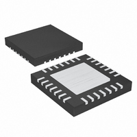
MAX1192ETI+ Maxim Integrated Products, MAX1192ETI+ Datasheet - Page 19

MAX1192ETI+
Manufacturer Part Number
MAX1192ETI+
Description
IC ADC 8BIT 22MSPS DUAL 28-TQFN
Manufacturer
Maxim Integrated Products
Datasheet
1.MAX1192ETI.pdf
(27 pages)
Specifications of MAX1192ETI+
Number Of Bits
8
Sampling Rate (per Second)
22M
Data Interface
Parallel
Number Of Converters
2
Voltage Supply Source
Single Supply
Operating Temperature
-40°C ~ 85°C
Mounting Type
Surface Mount
Package / Case
28-WFQFN Exposed Pad
Number Of Adc Inputs
2
Conversion Rate
22 MSPs
Resolution
8 bit
Input Type
Differential
Interface Type
Parallel
Voltage Reference
Internal 2.048 V or External
Supply Voltage (max)
3.6 V
Supply Voltage (min)
2.7 V
Maximum Power Dissipation
1667 mW
Maximum Operating Temperature
+ 85 C
Mounting Style
SMD/SMT
Minimum Operating Temperature
- 40 C
Lead Free Status / RoHS Status
Lead free / RoHS Compliant
Table 2. Output Codes vs. Input Voltage
Table 3. Power Logic
heavy capacitive loads. To improve the dynamic perfor-
mance of the MAX1192, add 100Ω resistors in series
with the digital outputs close to the MAX1192. Refer to
the MAX1193 Evaluation Kit schematic for an example
of the digital outputs driving a digital buffer through
100Ω series resistors.
The MAX1192 has four power modes that are con-
trolled with PD0 and PD1. Four power modes allow the
MAX1192 to efficiently use power by transitioning to a
low-power state when conversions are not required
(Table 3).
Shutdown mode offers the most dramatic power sav-
ings by shutting down all the analog sections of the
MAX1192 and placing the outputs in tri-state. The
DIFFERENTIAL INPUT VOLTAGE
PD0
0
0
1
1
V
V
V
V
-V
-V
-V
REF
REF
REF
REF
(IN+ - IN-)
REF
REF
REF
PD1
0
1
0
1
Ultra-Low-Power, 22Msps, Dual 8-Bit ADC
×
×
×
×
×
×
×
127
128
126
128
128
128
______________________________________________________________________________________
128
127
128
128
128
0
1
1
Normal Operating
POWER MODE
Power Modes (PD0, PD1)
Shutdown
Standby
Idle
DIFFERENTIAL INPUT
(+ full scale - 1 LSB)
(+ full scale - 2 LSB)
(- full scale + 1 LSB)
- 128 (- full scale)
0 (bipolar zero)
ADC
(LSB)
+127
+126
-127
Off
Off
On
On
+1
-1
REFERENCE
INTERNAL
Off
On
On
On
wake-up time from shutdown mode is dominated by the
time required to charge the capacitors at REFP, REFN,
and COM. In internal reference mode and buffered
external reference mode, the wake-up time is typically
20µs. When operating in the unbuffered external refer-
ence mode, the wake-up time is dependent on the
external reference drivers. When the outputs transition
from tri-state to on, the last converted word is placed
on the digital outputs.
In standby mode, the reference and clock distribution
circuits are powered up, but the pipeline ADCs are
unpowered and the outputs are in tri-state. The wake-
up time from standby mode is dominated by the 5.4µs
required to activate the pipeline ADCs. When the out-
puts transition from tri-state to on, the last converted
word is placed on the digital outputs.
OFFSET BINARY
1111 1111
1111 1110
1000 0001
1000 0000
0111 1111
0000 0001
0000 0000
(D7–D0)
CLOCK DISTRIBUTION
Off
On
On
On
OUTPUT DECIMAL CODE
255
254
129
128
127
1
0
OUTPUTS
Tri-state
Tri-state
Tri-state
On
19


