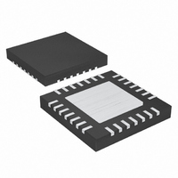
MAX1192ETI+ Maxim Integrated Products, MAX1192ETI+ Datasheet - Page 18

MAX1192ETI+
Manufacturer Part Number
MAX1192ETI+
Description
IC ADC 8BIT 22MSPS DUAL 28-TQFN
Manufacturer
Maxim Integrated Products
Datasheet
1.MAX1192ETI.pdf
(27 pages)
Specifications of MAX1192ETI+
Number Of Bits
8
Sampling Rate (per Second)
22M
Data Interface
Parallel
Number Of Converters
2
Voltage Supply Source
Single Supply
Operating Temperature
-40°C ~ 85°C
Mounting Type
Surface Mount
Package / Case
28-WFQFN Exposed Pad
Number Of Adc Inputs
2
Conversion Rate
22 MSPs
Resolution
8 bit
Input Type
Differential
Interface Type
Parallel
Voltage Reference
Internal 2.048 V or External
Supply Voltage (max)
3.6 V
Supply Voltage (min)
2.7 V
Maximum Power Dissipation
1667 mW
Maximum Operating Temperature
+ 85 C
Mounting Style
SMD/SMT
Minimum Operating Temperature
- 40 C
Lead Free Status / RoHS Status
Lead free / RoHS Compliant
provide lowest possible jitter. Any significant aperture
jitter would limit the SNR performance of the on-chip
ADCs as follows:
where f
t
Clock jitter is especially critical for undersampling
applications. The clock input should always be consid-
ered as an analog input and routed away from any ana-
log input or other digital signal lines. The MAX1192
clock input operates with a V
and accepts a 50% ±10% duty cycle (see Typical
Operating Characteristics ).
Figure 5 shows the relationship between the clock, ana-
log inputs, A/B indicator, and the resulting output data.
Channel A (CHA) and channel B (CHB) are simultane-
ously sampled on the rising edge of the clock signal
(CLK) and the resulting data is multiplexed at the out-
put. CHA data is updated on the rising edge and CHB
data is updated on the falling edge of the CLK. The A/B
indicator follows CLK with a typical delay time of 6ns
and remains high when CHA data is updated and low
when CHB data is updated. Including the delay
through the output latch, the total clock-cycle latency is
5 clock cycles for CHA and 5.5 clock cycles for CHB.
Ultra-Low-Power, 22Msps, Dual 8-Bit ADC
Figure 5. System Timing Diagram
18
AJ
CHB
D0–D7
is the time of the aperture jitter.
CLK
CHA
t
t
DA/B
______________________________________________________________________________________
A/B
DOB
SNR
IN
represents the analog input frequency and
=
t
CL
CHB
D0B
20
t
CLK
System Timing Requirements
×
t
CH
CHA
D1A
log
⎛
⎜
⎝
2
t
DOA
CHB
D1B
×
DD
π
/2 voltage threshold
×
5 CLOCK-CYCLE LATENCY (CHA), 5.5 CLOCK-CYCLE LATENCY (CHB)
1
CHA
D2A
f
IN
×
t
CHB
D2B
AJ
⎞
⎟
⎠
CHA
D3A
CHB
D3B
D0–D7 and A/B are TTL/CMOS-logic compatible. The
digital output coding is offset binary (Table 2, Figure 6).
The capacitive load on the digital outputs D0–D7
should be kept as low as possible (<15pF) to avoid
large digital currents feeding back into the analog por-
tion of the MAX1192 and degrading its dynamic perfor-
mance. Buffers on the digital outputs isolate them from
Figure 6. Transfer Function
1111 1111
1111 1110
1111 1101
1000 0001
1000 0000
0111 1111
0000 0011
0000 0010
0000 0001
0000 0000
CHA
D4A
-128
CHB
D4B
-127
1LSB =
-126 -125
Channel Data Indicator (A/ B B )
Digital Output Data (D0–D7),
2 x V
V
CHA
D5A
256
REF
REF
INPUT VOLTAGE (LSB)
-1
CHB
D5B
(COM)
0
+1
V
REF
CHA
D6A
V
= V
REF
REFP
+125
- V
+126
CHB
D6B
REFN
+127
+128
(COM)


