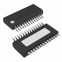
MAX1091BEEI+ Maxim Integrated Products, MAX1091BEEI+ Datasheet

MAX1091BEEI+
Specifications of MAX1091BEEI+
Related parts for MAX1091BEEI+
MAX1091BEEI+ Summary of contents
Page 1
... QSOP -40°C to +85°C MAX1091BEEI 28 QSOP Ordering Information continued at end of data sheet. ________________________________________________________________ Maxim Integrated Products For pricing, delivery, and ordering information, please contact Maxim/Dallas Direct! at 1-888-629-4642, or visit Maxim’s website at www.maxim-ic.com. o 10-Bit Resolution, ±0.5 LSB Linearity o +3V Single-Supply Operation o User-Adjustable Logic Level (+1.8V to +3.6V) o Internal +2 ...
Page 2
ADCs with +2.5V Reference and Parallel Interface ABSOLUTE MAXIMUM RATINGS V to GND ..............................................................-0. GND.........................................................-0.3V to +6V LOGIC CH0–CH7, COM to GND ............................-0. REF, REFADJ to GND ................................-0.3V to ...
Page 3
ADCs with +2.5V Reference and Parallel Interface ELECTRICAL CHARACTERISTICS (continued +2.7V to +3.6V, COM = GND, REFADJ = V DD LOGIC cycle unless otherwise noted. Typical ...
Page 4
ADCs with +2.5V Reference and Parallel Interface ELECTRICAL CHARACTERISTICS (continued +2.7V to +3.6V, COM = GND, REFADJ = V DD LOGIC cycle unless otherwise noted. Typical ...
Page 5
ADCs with +2.5V Reference and Parallel Interface TIMING CHARACTERISTICS (continued +2.7V to +3.6V, COM = GND, REFADJ = V DD LOGIC cycle unless otherwise noted. Typical ...
Page 6
ADCs with +2.5V Reference and Parallel Interface ( +3V +2.500V LOGIC REF INTEGRAL NONLINEARITY vs. OUTPUT CODE 0.4 0.3 0.2 0.1 0 -0.1 -0.2 -0.3 -0.4 0 200 400 ...
Page 7
ADCs with +2.5V Reference and Parallel Interface ( +3V +2.500V LOGIC REF INTERNAL REFERENCE VOLTAGE vs. SUPPLY VOLTAGE 2.53 2.52 2.51 2.50 2.49 2.48 2.7 3.0 3.3 V (V) ...
Page 8
ADCs with +2.5V Reference and Parallel Interface PIN NAME MAX1091 MAX1093 1 1 HBEN D1/D9 9 ...
Page 9
ADCs with +2.5V Reference and Parallel Interface Detailed Description Converter Operation The MAX1091/MAX1093 ADCs use a successive- approximation (SAR) conversion technique and an input track/hold (T/H) stage to convert an analog input signal to a 10-bit ...
Page 10
ADCs with +2.5V Reference and Parallel Interface 10-BIT CAPACITIVE DAC REF INPUT C HOLD MUX ZERO – + CH0 CH1 12pF CH2 R IN 800Ω CH3 C SWITCH HOLD CH4 TRACK AT THE SAMPLING INSTANT, CH5 ...
Page 11
ADCs with +2.5V Reference and Parallel Interface conversion. The sampling interval occurs at the end of the acquisition interval. The ACQMOD (acquisition mode) bit in the input control byte (Table 1) offers two options for acquiring ...
Page 12
ADCs with +2.5V Reference and Parallel Interface CSWS CONTROL D7–D0 BYTE ACQMOD = "0" HIGH-Z INT RD HBEN HIGH-Z DOUT Figure 4. Conversion Timing Using Internal Acquisition ...
Page 13
ADCs with +2.5V Reference and Parallel Interface Selecting Clock Mode The MAX1091/MAX1093 operate with either an internal or an external clock. Control bits D6 and D7 select either internal or external clock mode. The parts retain ...
Page 14
ADCs with +2.5V Reference and Parallel Interface ACQUISITION STARTS CLK ACQMOD = "1" ACQUISITION STARTS CLK ACQMOD = "1" Figure 6b. External Clock and WR Timing (External Acquisition Mode) Table ...
Page 15
ADCs with +2.5V Reference and Parallel Interface Table 4. Channel Selection for Pseudo-Differential Operation (SGL/DIF = ...
Page 16
ADCs with +2.5V Reference and Parallel Interface When applying an external reference to REF, disable the internal reference buffer by connecting REFADJ The DC input resistance at REF is 25kΩ. DD Therefore, an ...
Page 17
ADCs with +2.5V Reference and Parallel Interface Table 6. Full-Scale and Zero-Scale for Unipolar and Bipolar Operation UNIPOLAR MODE Full Scale Zero Scale — sion cycles, and 2 read cycles. This assumes that the results of ...
Page 18
ADCs with +2.5V Reference and Parallel Interface CLK WR RD HBEN CONTROL D7–D0 D9–D8 D7–D0 BYTE LOW HIGH BYTE BYTE STATE ACQUISITION SAMPLING INSTANT Figure 10. Timing Diagram for Fastest Conversion Total ...
Page 19
ADCs with +2.5V Reference and Parallel Interface CLK V LOGIC MAX1091 REF µP WR REFADJ CONTROL INPUTS RD HBEN INT CH7 D7 CH6 CH5 D6 CH4 D5 CH3 D4 CH2 D3 CH1 D2 ...
Page 20
... Maxim cannot assume responsibility for use of any circuitry other than circuitry entirely embodied in a Maxim product. No circuit patent licenses are implied. Maxim reserves the right to change the circuitry and specifications without notice at any time. 20 ____________________Maxim Integrated Products, 120 San Gabriel Drive, Sunnyvale, CA 94086 408-737-7600 © 2002 Maxim Integrated Products Printed USA is a registered trademark of Maxim Integrated Products ...


