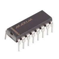
MX7705EPE+ Maxim Integrated Products, MX7705EPE+ Datasheet - Page 29

MX7705EPE+
Manufacturer Part Number
MX7705EPE+
Description
IC ADC 16BIT 2CH 16-DIP
Manufacturer
Maxim Integrated Products
Datasheet
1.MX7705EPE.pdf
(33 pages)
Specifications of MX7705EPE+
Number Of Bits
16
Sampling Rate (per Second)
500
Data Interface
MICROWIRE™, QSPI™, Serial, SPI™
Number Of Converters
1
Voltage Supply Source
Single Supply
Operating Temperature
-40°C ~ 85°C
Mounting Type
Through Hole
Package / Case
16-DIP (0.300", 7.62mm)
Lead Free Status / RoHS Status
Lead free / RoHS Compliant
Next, an internally generated voltage (V
applied across AIN+ and AIN-. This condition results in
the full-scale calibration.
Start self-calibration by setting MD1 = 0, MD0 = 1, and
FSYNC = 0 in the setup register. Self-calibration com-
pletes in 6 x 1/output data rate. The MD1 and MD0 bits
both return to zero at the end of calibration. The device
returns to normal acquisition mode and performs a con-
version, which completes in 3 x 1/output data rate after
the self-calibration sequence.
The DRDY output goes high at the start of calibration
and falls low when the calibration is complete and the
next conversion result is valid in the data register. The
total time for self-calibration and one conversion (time
until DRDY goes low) is 9 x 1/output data rate. If DRDY
is low before or goes low during the calibration com-
mand write to the setup register, DRDY takes up to one
additional modulator cycle (128/f
indicate a calibration or conversion in progress.
System calibration compensates for offset and gain
errors for the entire analog signal path including the
ADC, signal conditioning, and signal source. System
calibration is a two-step process and requires individ-
ual zero-scale and full-scale calibrations on the select-
ed channel at a specified PGA gain. Recalibration is
recommended with changes in ambient temperature,
supply voltage, bipolar/unipolar mode, PGA gain, and
output data rate. Before starting calibration, set the
PGA gain and the desired channel.
Set the zero-scale reference point across AIN+ and AIN-.
Start the zero-scale calibration by setting MD1 = 1, MD0
= 0, and FSYNC = 0 in the setup register. When zero-
scale calibration is complete (3 x 1/output data rate),
MD1 and MD0 both return to zero. DRDY goes high at the
start of the zero-scale system calibration and returns low
when there is a valid word in the data register (4 x 1/out-
put data rate). The time until DRDY goes low is com-
prised of one zero-scale calibration sequence (3 x
1/output data rate) and one conversion on the AIN volt-
age (1 x 1/output data rate). If DRDY is low before or
goes low during the calibration command write to the
setup register, DRDY takes up to one additional modula-
tor cycle (128/f
tion or conversion in progress.
CLKIN
______________________________________________________________________________________
) to return high to indicate a calibra-
CLKIN
System Calibration
) to return high to
REF
16-Bit, Low-Power, 2-Channel,
/ GAIN) is
After performing a zero-scale calibration, connect the
analog inputs to the full-scale voltage level (V
GAIN). Perform a full-scale calibration by setting MD1 =
1 and MD0 = 1. After 3 x 1/output data rate, MD1 and
MD0 both return to zero at the completion of full-scale
calibration. DRDY goes high at the beginning of cali-
bration and returns low after calibration is complete
and new data is in the data register (4 x 1/output data
rate). The time until DRDY goes low is comprised of
one full-scale calibration sequence (3 x 1/output data
rate) and one conversion on the AIN voltage (1 x 1/out-
put data rate). If DRDY is low before or goes low during
the calibration-command write to the setup register,
DRDY takes up to one additional modulator cycle
(128/f
conversion in progress.
In bipolar mode, the midpoint (zero scale) and positive
full scale of the transfer function are used to calculate the
calibration coefficients of the gain and offset registers. In
unipolar mode, system calibration is performed using the
two endpoints of the transfer function (Figures 4 and 5).
The MX7705 includes a power-down mode to save
power. Select power-down mode by setting PD = 1 in
the communications register. The PD bit does not affect
the serial interface or the status of the DRDY line. While
in power-down mode, the MX7705 retains the contents
of all of its registers. Placing the part in power-down
mode reduces current consumption to 2µA (typ) when
in external clock mode and with CLKIN connected to
V
power-down mode, then DRDY remains high until the
part returns to normal operation mode and new data is
available in the data register. If DRDY is low before the
part enters power-down mode, indicating new data in
the data register, the data register can be read during
power-down mode. DRDY goes high at the end of this
read operation. If the new data remains unread, DRDY
stays low until the MX7705 is taken out of power-down
mode and resumes data conversion. Resume normal
operation by setting PD = 0. The device begins a new
conversion with a result appearing in 3 x 1/output data
rate + t
0. If the clock is stopped during power-down mode,
allow sufficient time for the clock to start up before
resuming conversion.
If CLKDIS = 0, CLKOUT remains active during power-
down mode to provide a clock source for other devices
in the system.
DD
or GND. If DRDY is high before the part enters
CLKIN
P
, where t
) to return high to indicate a calibration or
Sigma-Delta ADC
P
= 2000 x 1/f
Power-Down Modes
CLKIN
, after PD is set to
REF
29
/


