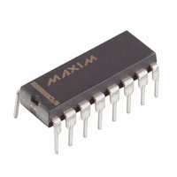
MX7705EPE+ Maxim Integrated Products, MX7705EPE+ Datasheet - Page 26

MX7705EPE+
Manufacturer Part Number
MX7705EPE+
Description
IC ADC 16BIT 2CH 16-DIP
Manufacturer
Maxim Integrated Products
Datasheet
1.MX7705EPE.pdf
(33 pages)
Specifications of MX7705EPE+
Number Of Bits
16
Sampling Rate (per Second)
500
Data Interface
MICROWIRE™, QSPI™, Serial, SPI™
Number Of Converters
1
Voltage Supply Source
Single Supply
Operating Temperature
-40°C ~ 85°C
Mounting Type
Through Hole
Package / Case
16-DIP (0.300", 7.62mm)
Lead Free Status / RoHS Status
Lead free / RoHS Compliant
Drive RESET low to reset the MX7705 to power-on reset
status. DRDY goes high and all communication to the
MX7705 is ignored while RESET is low. Upon releasing
RESET, the device must be reconfigured to begin a con-
version. The device returns to waiting for a write to the
communication register after a reset has been performed.
Perform a calibration sequence following a reset for
accurate conversions.
The MX7705 clock generator continues to run when
RESET is pulled low. This allows any device running from
CLKOUT to be uninterrupted when the device is in reset.
The recommended frequency range of the external clock
is 400kHz to 5MHz. The output data rate and first notch
frequency are dependent on the decimation rate of the
digital filter. Table 14 shows the available decimation
rates of the digital filter. The output data rate and filter first
notch is calculated using the following formula:
(if CLKDIV = 1)
(if CLKDIV = 0)
Note: First-notch filter frequency = output data rate.
At power-on reset, the MX7705 expects a write to the
communications register. Writing to the communica-
tions register selects the acquisition channel, read/write
operation for the next register, power-down/normal
mode, and address of the following register to be
accessed. The MX7705 has six user-accessible regis-
ters, which control the function of the device and allow
the result to be read. Write to the communications reg-
ister before accessing any other registers.
16-Bit, Low-Power, 2-Channel,
Sigma-Delta ADC
26
output data rate
Selecting Custom Output Data Rates and
______________________________________________________________________________________
output data rate
=
128
=
Performing a Conversion
128
×
First-Notch Frequency
Decimation Rate
×
f
CLKIN
Decimation Rate
f
CLKIN
×
Reset
0 5
.
Writing to the clock and setup registers after configuring
and initializing the host processor serial port sets up the
MX7705. Use self- or system calibrations to minimize off-
set and gain errors (see the Calibration section for more
details). Set FSYNC = 0 to begin calibration or conver-
sion. The MX7705 performs free-running acquisitions
when FSYNC is low (see the Using FSYNC section). The
µC can poll the DRDY bit of the communications register
and read the data register when the DRDY bit returns a
0. For hardware polling, the DRDY output goes low when
the new data is valid in the data register.
The data register can be read multiple times while the
next conversion takes place.
The flow diagram in Figure 11 shows an example
sequence required to perform a conversion on channel
1 (AIN1+ / AIN1-) after a power-on reset.
Table 14. Filter Select and Decimation Rate
CLK
0
0
0
0
1
1
1
1
FS1
0
0
1
1
0
0
1
1
FS0
0
1
0
1
0
1
0
1
DECIMATION RATE
391
313
384
320
78
39
77
38


