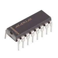
MX7705EPE+ Maxim Integrated Products, MX7705EPE+ Datasheet - Page 28

MX7705EPE+
Manufacturer Part Number
MX7705EPE+
Description
IC ADC 16BIT 2CH 16-DIP
Manufacturer
Maxim Integrated Products
Datasheet
1.MX7705EPE.pdf
(33 pages)
Specifications of MX7705EPE+
Number Of Bits
16
Sampling Rate (per Second)
500
Data Interface
MICROWIRE™, QSPI™, Serial, SPI™
Number Of Converters
1
Voltage Supply Source
Single Supply
Operating Temperature
-40°C ~ 85°C
Mounting Type
Through Hole
Package / Case
16-DIP (0.300", 7.62mm)
Lead Free Status / RoHS Status
Lead free / RoHS Compliant
When FSYNC = 1, the digital filter and analog modula-
tor are in a reset state, inhibiting normal operation. Set
FSYNC = 0 to begin calibration or conversion.
When configured for normal operation (MD0 and MD1
set to 0), DRDY goes low 3 x 1/output data rate after
FSYNC goes low to indicate that the new conversion
result is ready to be read from the data register. DRDY
returns high when a read operation on the data register
is complete. As long as FSYNC remains low, the
MX7705 performs free-running conversions with the
data registers updating at the output data rate. If the
valid data is not read before the next conversion result
is ready, DRDY returns high for 500 x 1/f
going low again to indicate a new conversion. Set
FSYNC = 1 to stop converting data.
If FSYNC goes high while DRDY is low (indicating that
valid data has not yet been read from the data regis-
ter), DRDY does not reset high. DRDY remains low until
the new data is read from the data register or until
FSYNC goes low to begin a new conversion.
Table 15 provides the duration-to-mode bits and dura-
tion-to-DRDY for each calibration sequence. Duration-to-
mode bits provide the time required for the calibration
sequence to complete (MD1 and MD0 return to 0).
Duration-to-DRDY provides the time until the first conver-
sion result is valid in the data register (DRDY goes low).
The pipeline delay necessary to ensure that the first
conversion result is valid is t
When selecting self-calibration (MD1 = 0, MD0 = 1),
DRDY goes low 9 x 1/output data rate + t
goes low (or after a write operation to the setup register
with MD1 = 0 and MD0 = 1 is performed while FSYNC
is already low) to indicate new data in the data register.
The pipeline delay required to ensure that the first con-
version result is valid is t
16-Bit, Low-Power, 2-Channel,
Sigma-Delta ADC
Table 15. Calibration Sequences
* Duration-to-mode bits represents the completion of the calibration sequence.
** Duration to DRDY represents the time at which a new conversion result is available in the data register.
28
Self-calibration (0,1)
Zero-scale system calibration (1,0)
Full-scale system calibration (1,1)
______________________________________________________________________________________
CALIBRATION TYPE
(MD1, MD0)
P
(t
P
P
= 2000 x 1/f
(t
P
= 2000 x 1/f
Internal zero-scale calibration at
selected gain + internal full-scale
calibration at selected gain
Zero-scale calibration on AIN at
selected gain
Full-scale calibration on AIN at
selected gain
CALIBRATION SEQUENCE
Using FSYNC
CLKIN
P
CLKIN
after FSYNC
CLKIN
).
before
).
When zero-scale or full-scale calibration is selected,
DRDY goes low 4 x 1/output data rate + t
goes low (or while the zero-scale or full-scale calibra-
tion command is issued when FSYNC is already low) to
indicate new data in the data register (see the
Calibration section).
To compensate for errors introduced by temperature
variations or system DC offsets, perform an on-chip cal-
ibration. Select calibration options by writing to the
MD1 and MD0 bits in the setup register (Table 9).
Calibration removes gain and offset errors from the
device and/or the system. Recalibrate with changes in
ambient temperature, supply voltage, bipolar/unipolar
mode, PGA gain, and output data rate.
The MX7705 offers two calibration modes, self-calibra-
tion and system calibration. The channels of the
MX7705 are independently calibrated (Table 8). The
calibration coefficients resulting from a calibration
sequence on a selected channel are stored in the corre-
sponding offset and gain-register pair.
Self- and system calibration automatically calculate the
offset and gain coefficients, which are written to the off-
set and gain registers. These offset and gain coeffi-
cients provide offset and gain-error correction for the
specified channel.
Self-calibration compensates for offset and gain errors
internal to the ADC. Prior to calibration, set the PGA gain,
unipolar/bipolar mode, and input channel setting. During
self-calibration, AIN+ and AIN- of the selected channel
are internally shorted together. The ADC calibrates this
condition as the zero-scale output level. For bipolar
mode, this zero-scale point is the midscale of the bipolar
transfer function.
DURATION-TO-MODE
6 x 1/output data rate
3 x 1/output data rate
3 x 1/output data rate
BITS*
9 x 1/output data rate + t
4 x 1/output data rate + t
4 x 1/output data rate + t
DURATION TO DRDY**
Self-Calibration
P
Calibration
after FSYNC
P
P
P


