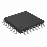
MAX1498ECJ+ Maxim Integrated Products, MAX1498ECJ+ Datasheet - Page 15

MAX1498ECJ+
Manufacturer Part Number
MAX1498ECJ+
Description
IC ADC 4 1/2DIG W/LED DVR 32TQFP
Manufacturer
Maxim Integrated Products
Datasheet
1.MAX1496EAI.pdf
(24 pages)
Specifications of MAX1498ECJ+
Number Of Bits
4.5 Digit
Sampling Rate (per Second)
5
Number Of Converters
1
Power Dissipation (max)
1.65W
Voltage Supply Source
Analog and Digital
Operating Temperature
-40°C ~ 85°C
Mounting Type
Surface Mount
Package / Case
32-LQFP
Lead Free Status / RoHS Status
Lead free / RoHS Compliant
For external-reference operation, set INTREF to GND.
REF+ and REF- are fully differential. For a valid exter-
nal-reference input, V
Bypass REF+ and REF- with a 0.1µF or greater capaci-
tor to GND in external-reference mode.
Figure 8 shows the MAX1447/MAX1496/MAX1498 oper-
ating with an external differential reference. In this fig-
ure, REF- is connected to the top of the strain gauge
and REF+ is connected to the midpoint of the resistor-
divider of the supply.
Figure 9 shows the MAX1447/MAX1496/MAX1498 oper-
ating with an external single-ended reference. In this
figure, REF- is connected to GND and REF+ is driven
with an external 2.048V reference. Bypass REF+ to
GND with a 0.47µF capacitor.
At power-up, the digital filter and modulator circuits reset.
The MAX1447/MAX1498 allows 6s for the reference to
stabilize before performing enhanced offset calibration.
During these 6s, the MAX1447/MAX1498 display 1.2V
to 1.5V when a stable reference is detected. If a valid
reference is not found, the MAX1447/MAX1498 time out
after 6s and begin enhanced offset calibration.
Enhanced offset calibration typically lasts 2s. The
MAX1447/MAX1498 begin converting after enhanced
offset calibration.
Figure 8. Strain-Gauge Application with the MAX1447/MAX1496/
MAX1498
DUMMY
ACTIVE
GAUGE
GAUGE
0.1µF
R
REF
0.1µF
R
R
Applications Information
0.1µF
0.1µF
0.1µF
______________________________________________________________________________________
REF+
4.7µF
REF+
REF-
AIN+
AIN-
must be greater than V
AV
DD
ANALOG SUPPLY
MAX1447
MAX1496
MAX1498
3.5- and 4.5-Digit, Single-Chip ADCs
FERRITE
GND
BEAD
Power-On Reset
DV
DD
0.1µF
4.7µF
REF-
.
The MAX1447/MAX1496/MAX1498 offer on-chip offset
calibration. The device offset calibrates during every con-
version cycle.
Enhanced offset calibration is a more accurate calibra-
tion method that is needed in the case of the ±200mV
range and 4.5-digit resolution. In addition to enhanced
offset calibration at power-up, the MAX1447 performs
enhanced calibration on demand by connecting HOLD
to AV
The MAX1447/MAX1496/MAX1498 feature peak-detec-
tion circuitry. When activated (PEAK connected to
AV
MAX1496), the devices display only the highest voltage
measured to the LED.
First, the current ADC result is displayed. The new ADC
conversion result is compared to the current result. If the
new value is larger than the previous peak value, the
new value is displayed. If the new value is less than the
previous peak value, the display remains unchanged.
Connect PEAK to GND to clear the peak value and dis-
able the peak function.
Figure 9. Thermocouple Application with the MAX1447/MAX1496/
MAX1498
DD
DD
MAX6062
THERMOCOUPLE
for the MAX1498/MAX1447 or to V
JUNCTION
+5V
for > 2s.
with LED Drivers
+2.048V
0.1µF
Enhanced Offset Calibration
0.47µF
AIN+
AIN-
REF+
REF-
GND
Offset Calibration
MAX1447
MAX1496
MAX1498
(MAX1447 Only)
DD
for the
Peak
15


