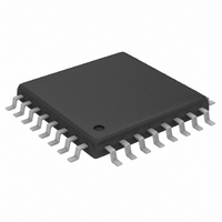
MAX1498ECJ+ Maxim Integrated Products, MAX1498ECJ+ Datasheet - Page 14

MAX1498ECJ+
Manufacturer Part Number
MAX1498ECJ+
Description
IC ADC 4 1/2DIG W/LED DVR 32TQFP
Manufacturer
Maxim Integrated Products
Datasheet
1.MAX1496EAI.pdf
(24 pages)
Specifications of MAX1498ECJ+
Number Of Bits
4.5 Digit
Sampling Rate (per Second)
5
Number Of Converters
1
Power Dissipation (max)
1.65W
Voltage Supply Source
Analog and Digital
Operating Temperature
-40°C ~ 85°C
Mounting Type
Surface Mount
Package / Case
32-LQFP
Lead Free Status / RoHS Status
Lead free / RoHS Compliant
The MAX1447/MAX1496/MAX1498 allow for full deci-
mal-point control and feature leading-zero suppression.
Use the DPON, DPSET1, and DPSET2 bits in the con-
trol register to set the value of the decimal point (Tables
2 and 3). The MAX1447/MAX1496/MAX1498 overrange
and underrange display is shown in Table 4.
The MAX1447/MAX1496/MAX1498 include a leading-
zero suppression circuitry to turn off unnecessary zeros.
For example, when DPSET1 and DPSET2 = [0,0], 0.0 is
displayed instead of 000.0. This feature saves a substan-
tial amount of power from being wasted.
The MAX1447/MAX1496/MAX1498 also include an
interdigit blanking circuitry. Without this feature, it is
possible to see a faint digit next to a digit that is com-
pletely on. The interdigit blanking circuitry prevents
bleeding over into the next digit for a short period of
time. The typical interdigit blanking time is 4µs.
3.5- and 4.5-Digit, Single-Chip ADCs
with LED Drivers
Table 2. Decimal-Point Control Table—MAX1447/MAX1498
Table 3. Decimal-Point Control Table—MAX1496
Table 4. LED During Overrange and
Underrange Conditions
14
X = Don’t care.
CONDITION
Underrange
Overrange
______________________________________________________________________________________
DPON
0
0
0
0
1
1
1
1
DPSET1
0
0
1
1
DPSET1
Leading-Zero Suppression
MAX1496
-
1
0
0
1
1
0
0
1
1
1
---
---
Decimal-Point Control
Interdigit Blanking
DPSET2
MAX1447/MAX1498
0
1
0
1
DPSET2
0
1
0
1
0
1
0
1
-
1
1
----
----
DISPLAY OUTPUT
DISPLAY OUTPUT
The MAX1447/MAX1496/MAX1498 reference sets the
full-scale range of the ADC transfer function. With a
nominal 2.048V reference, the ADC full-scale range is
±2V with RANGE = GND. With RANGE = DV
(MAX1447/MAX1498) or V
range is ±200mV. A decreased reference voltage
decreases full-scale range (see the Transfer Functions
section).
The MAX1447/MAX1496/MAX1498 accept either an
external reference or an internal reference (INTREF).
The INTREF logic selects the reference mode.
For internal-reference operation, set INTREF to DV
(MAX1447/MAX1498) or V
to GND, and bypass REF+ to GND with a 4.7µF capaci-
tor. The internal reference provides a nominal 2.048V
source between REF+ and GND. The internal-reference
temperature coefficient is typically 40ppm/°C.
1888.8
188.88
18.888
1.8888
18888
18888
18888
18888
188.8
18.88
1.888
1888
DD
DD
ZERO INPUT READING
ZERO INPUT READING
(MAX1496), connect REF-
(MAX1496), the full-scale
0.0000
0.000
0.00
0.0
0
0
0
0
0.000
0.00
0.0
0
Reference
DD
DD


