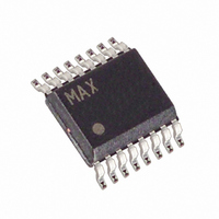
MAX1248BEEE+ Maxim Integrated Products, MAX1248BEEE+ Datasheet - Page 20

MAX1248BEEE+
Manufacturer Part Number
MAX1248BEEE+
Description
IC ADC 10BIT SERIAL 16-QSOP
Manufacturer
Maxim Integrated Products
Datasheet
1.MAX1249BCPE.pdf
(24 pages)
Specifications of MAX1248BEEE+
Number Of Bits
10
Sampling Rate (per Second)
133k
Data Interface
MICROWIRE™, QSPI™, Serial, SPI™
Number Of Converters
1
Power Dissipation (max)
3.6mW
Voltage Supply Source
Single Supply
Operating Temperature
-40°C ~ 85°C
Mounting Type
Surface Mount
Package / Case
16-SSOP (0.150", 3.90mm Width)
Number Of Adc Inputs
4
Architecture
SAR
Conversion Rate
133 KSPs
Resolution
10 bit
Input Type
Voltage
Interface Type
4-Wire (SPI, QSPI, MICROWIRE, TMS320)
Voltage Reference
2.5 V
Supply Voltage (max)
5.25 V
Supply Voltage (min)
2.7 V
Maximum Power Dissipation
842 mW
Maximum Operating Temperature
+ 85 C
Mounting Style
SMD/SMT
Minimum Operating Temperature
- 40 C
Lead Free Status / RoHS Status
Lead free / RoHS Compliant
Figure 20 shows an application circuit to interface the
MAX1248/MAX1249 to the TMS320 in external clock
mode. The timing diagram for this interface circuit is
shown in Figure 21.
Use the following steps to initiate a conversion in the
MAX1248/MAX1249 and to read the results:
1) The TMS320 should be configured with CLKX
2) The MAX1248/MAX1249’s CS pin is driven low by
3) An 8-bit word (1XXXXX11) should be written to the
4) The MAX1248/MAX1249’s SSTRB output is moni-
+2.7V to +5.25V, Low-Power, 4-Channel,
Serial 10-Bit ADCs in QSOP-16
20
Figure 19. MAX1248/MAX1249 QSPI Connections External Reference
(transmit clock) as an active-high output clock and
CLKR (TMS320 receive clock) as an active-high
input clock. CLKX and CLKR on the TMS320 are
tied together with the MAX1248/MAX1249’s SCLK
input.
the TMS320’s XF_ I/O port, to enable data to be
clocked into the MAX1248/MAX1249’s DIN.
MAX1248/MAX1249 to initiate a conversion and
place the device into external clock mode. Refer to
Table 1 to select the proper XXXXX bit values for
your specific application.
tored via the TMS320’s FSR input. A falling edge on
the SSTRB output indicates that the conversion is in
progress and data is ready to be received from the
MAX1248/MAX1249.
______________________________________________________________________________________
+2.5V
0.1 F
ANALOG
INPUTS
0.1 F
TMS320LC3x Interface
1
2
3
4
5
6
7
8
V
CH0
CH1
CH2
CH3
COM
SHDN
VREF
DD
MAX1248
MAX1249
REFADJ
SSTRB
DGND
DOUT
AGND
SCLK
DIN
CS
10
16
15
14
13
12
11
9
CLOCK CONNECTIONS NOT SHOWN
5) The TMS320 reads in one data bit on each of the
6) Pull CS high to disable the MAX1248/MAX1249 until
Figure 20. MAX1248/MAX1249-to-TMS320 Serial Interface
next 16 rising edges of SCLK. These data bits rep-
resent the 10 + 2-bit conversion result followed by
four trailing bits, which should be ignored.
the next conversion is initiated.
1 F
TMS320LC3x
+3V
+3V
CLKX
CLKR
FSR
DX
DR
XF
SCK
PCS0
MOSI
MISO
MC683XX
(GND)
CS
SCLK
DIN
DOUT
SSTRB
MAX1249


