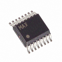
MAX1248BEEE+ Maxim Integrated Products, MAX1248BEEE+ Datasheet - Page 17

MAX1248BEEE+
Manufacturer Part Number
MAX1248BEEE+
Description
IC ADC 10BIT SERIAL 16-QSOP
Manufacturer
Maxim Integrated Products
Datasheet
1.MAX1249BCPE.pdf
(24 pages)
Specifications of MAX1248BEEE+
Number Of Bits
10
Sampling Rate (per Second)
133k
Data Interface
MICROWIRE™, QSPI™, Serial, SPI™
Number Of Converters
1
Power Dissipation (max)
3.6mW
Voltage Supply Source
Single Supply
Operating Temperature
-40°C ~ 85°C
Mounting Type
Surface Mount
Package / Case
16-SSOP (0.150", 3.90mm Width)
Number Of Adc Inputs
4
Architecture
SAR
Conversion Rate
133 KSPs
Resolution
10 bit
Input Type
Voltage
Interface Type
4-Wire (SPI, QSPI, MICROWIRE, TMS320)
Voltage Reference
2.5 V
Supply Voltage (max)
5.25 V
Supply Voltage (min)
2.7 V
Maximum Power Dissipation
842 mW
Maximum Operating Temperature
+ 85 C
Mounting Style
SMD/SMT
Minimum Operating Temperature
- 40 C
Lead Free Status / RoHS Status
Lead free / RoHS Compliant
Figure 13b shows the power consumption with
external-reference compensation in fast power-down,
with one and four channels converted. The external
4.7µF compensation requires a 75µs wait after power-up
with one dummy conversion. This circuit combines fast
multi-channel conversion with lowest power consumption
possible. Full power-down mode may provide increased
power
MAX1248/MAX1249 are inactive for long periods of time,
but where intermittent bursts of high-speed conversions
are required.
The MAX1248 can be used with an internal or external
reference voltage, whereas an external reference is
required for the MAX1249. An external reference can
be connected directly at VREF or at the REFADJ pin.
An internal buffer is designed to provide 2.5V at VREF
for both the MAX1248 and the MAX1249. The
MAX1248’s internally trimmed 1.21V reference is
buffered with a gain of 2.06. The MAX1249’s REFADJ
pin is also buffered with a gain of 2.06 to scale an
external 1.25V reference at REFADJ to 2.5V at VREF.
The MAX1248’s full-scale range with the internal refer-
ence is 2.5V with unipolar inputs and ±1.25V with bipo-
lar inputs. The internal-reference voltage is adjustable
to ±1.5% with the circuit of Figure 15.
Figure 13a. MAX1248 Supply Current vs. Conversion Rate,
FULLPD
savings
100
10
1
Internal and External References
0.01
Lowest Power at Higher Throughputs
R
CODE = 1010101000
LOAD
______________________________________________________________________________________
0.1
+2.7V to +5.25V, Low-Power, 4-Channel,
=
in
CONVERSION RATE (Hz)
4 CHANNELS
Internal Reference (MAX1248)
applications
1
10
1 CHANNEL
100
where
Serial 10-Bit ADCs in QSOP-16
1k
the
Figure 13b. MAX1248 Supply Current vs. Conversion Rate,
FASTPD
Figure 13c. Typical Reference-Buffer Power-Up Delay vs. Time
in Shutdown
10,000
1000
100
3.0
2.5
2.0
1.5
1.0
0.5
10
0
1
0.1
0
R
CODE = 1010101000
LOAD
1
=
0.01
TIME IN SHUTDOWN (sec)
10
CONVERSION RATE (Hz)
4 CHANNELS
100
0.1
1k
1 CHANNEL
10k
1
100k
1M
10
17


