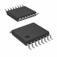
ADC108S022CIMT/NOPB National Semiconductor, ADC108S022CIMT/NOPB Datasheet - Page 16

ADC108S022CIMT/NOPB
Manufacturer Part Number
ADC108S022CIMT/NOPB
Description
ADC 10BIT 8CH 50-200KSPS
Manufacturer
National Semiconductor
Series
PowerWise®r
Datasheet
1.ADC108S022CIMTNOPB.pdf
(18 pages)
Specifications of ADC108S022CIMT/NOPB
Number Of Bits
10
Sampling Rate (per Second)
200k
Data Interface
DSP, MICROWIRE™, QSPI™, Serial, SPI™
Number Of Converters
1
Power Dissipation (max)
6.4mW
Voltage Supply Source
Analog and Digital
Operating Temperature
-40°C ~ 105°C
Mounting Type
Surface Mount
Package / Case
16-TSSOP (0.173", 4.40mm Width)
Number Of Elements
1
Resolution
10Bit
Architecture
SAR
Sample Rate
200KSPS
Input Polarity
Unipolar
Input Type
Voltage
Rated Input Volt
5.25V
Differential Input
No
Power Supply Requirement
Analog and Digital
Single Supply Voltage (typ)
3.3/5V
Single Supply Voltage (min)
2.7V
Single Supply Voltage (max)
5.25V
Dual Supply Voltage (typ)
Not RequiredV
Dual Supply Voltage (min)
Not RequiredV
Dual Supply Voltage (max)
Not RequiredV
Differential Linearity Error
±0.3LSB
Integral Nonlinearity Error
±0.3LSB
Operating Temp Range
-40C to 105C
Operating Temperature Classification
Industrial
Mounting
Surface Mount
Pin Count
16
Package Type
TSSOP
Input Signal Type
Single-Ended
For Use With
ADC108S022EVAL - BOARD EVALUATION FOR ADC108S022
Lead Free Status / RoHS Status
Lead free / RoHS Compliant
Other names
*ADC108S022CIMT
*ADC108S022CIMT/NOPB
ADC108S022CIMT
*ADC108S022CIMT/NOPB
ADC108S022CIMT
Available stocks
Company
Part Number
Manufacturer
Quantity
Price
Part Number:
ADC108S022CIMT/NOPB
Manufacturer:
TI/德州仪器
Quantity:
20 000
www.national.com
section shows the typical power consumption of the AD-
C108S022. To calculate the power consumption (P
multiply the fraction of time spent in the normal mode (t
the normal mode power consumption (P
tion of time spent in shutdown mode (t
shutdown mode power consumption (P
9.
2.2.3 Power Supply Noise Considerations
The charging of any output load capacitance requires current
from the digital supply, V
the supply to charge the output capacitance will cause voltage
variations on the digital supply. If these variations are large
enough, they could degrade SNR and SINAD performance of
the ADC. Furthermore, if the analog and digital supplies are
tied directly together, the noise on the digital supply will be
coupled directly into the analog supply, causing greater per-
formance degradation than would noise on the digital supply
alone. Similarly, discharging the output capacitance when the
digital output goes from a logic high to a logic low will dump
current into the die substrate, which is resistive. Load dis-
charge currents will cause "ground bounce" noise in the sub-
strate that will degrade noise performance if that current is
large enough. The larger the output capacitance, the more
current flows through the die substrate and the greater the
noise coupled into the analog channel.
The first solution to keeping digital noise out of the analog
supply is to decouple the analog and digital supplies from
each other or use separate supplies for them. To keep noise
out of the digital supply, keep the output load capacitance as
small as practical. If the load capacitance is greater than 50
pF, use a 100 Ω series resistor at the ADC output, located as
close to the ADC output pin as practical. This will limit the
FIGURE 9. Power Consumption Equation
D
. The current pulses required from
S
N
) as shown in
S
), and add the frac-
) multiplied by the
20164515
C
), simply
Figure
N
) by
16
charge and discharge current of the output capacitance and
improve noise performance. Since the series resistor and the
load capacitance form a low frequency pole, verify signal in-
tegrity once the series resistor has been added.
2.3 LAYOUT AND GROUNDING
Capacitive coupling between the noisy digital circuitry and the
sensitive analog circuitry can lead to poor performance. The
solution is to keep the analog circuitry separated from the
digital circuitry and the clock line as short as possible.
Digital circuits create substantial supply and ground current
transients. The logic noise generated could have significant
impact upon system noise performance. To avoid perfor-
mance degradation of the ADC108S022 due to supply noise,
do not use the same supply for the ADC108S022 that is used
for digital logic.
Generally, analog and digital lines should cross each other at
90° to avoid crosstalk. However, to maximize accuracy in high
resolution systems, avoid crossing analog and digital lines al-
together. It is important to keep clock lines as short as possi-
ble and isolated from ALL other lines, including other digital
lines. In addition, the clock line should also be treated as a
transmission line and be properly terminated.
The analog input should be isolated from noisy signal traces
to avoid coupling of spurious signals into the input. Any ex-
ternal component (e.g., a filter capacitor) connected between
the converter's input pins and ground or to the reference input
pin and ground should be connected to a very clean point in
the ground plane.
We recommend the use of a single, uniform ground plane and
the use of split power planes. The power planes should be
located within the same board layer. All analog circuitry (input
amplifiers, filters, reference components, etc.) should be
placed over the analog power plane. All digital circuitry and I/
O lines should be placed over the digital power plane. Fur-
thermore, all components in the reference circuitry and the
input signal chain that are connected to ground should be
connected together with short traces and enter the analog
ground plane at a single, quiet point.


