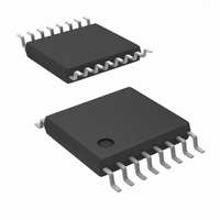
ADC108S022CIMT/NOPB National Semiconductor, ADC108S022CIMT/NOPB Datasheet - Page 14

ADC108S022CIMT/NOPB
Manufacturer Part Number
ADC108S022CIMT/NOPB
Description
ADC 10BIT 8CH 50-200KSPS
Manufacturer
National Semiconductor
Series
PowerWise®r
Datasheet
1.ADC108S022CIMTNOPB.pdf
(18 pages)
Specifications of ADC108S022CIMT/NOPB
Number Of Bits
10
Sampling Rate (per Second)
200k
Data Interface
DSP, MICROWIRE™, QSPI™, Serial, SPI™
Number Of Converters
1
Power Dissipation (max)
6.4mW
Voltage Supply Source
Analog and Digital
Operating Temperature
-40°C ~ 105°C
Mounting Type
Surface Mount
Package / Case
16-TSSOP (0.173", 4.40mm Width)
Number Of Elements
1
Resolution
10Bit
Architecture
SAR
Sample Rate
200KSPS
Input Polarity
Unipolar
Input Type
Voltage
Rated Input Volt
5.25V
Differential Input
No
Power Supply Requirement
Analog and Digital
Single Supply Voltage (typ)
3.3/5V
Single Supply Voltage (min)
2.7V
Single Supply Voltage (max)
5.25V
Dual Supply Voltage (typ)
Not RequiredV
Dual Supply Voltage (min)
Not RequiredV
Dual Supply Voltage (max)
Not RequiredV
Differential Linearity Error
±0.3LSB
Integral Nonlinearity Error
±0.3LSB
Operating Temp Range
-40C to 105C
Operating Temperature Classification
Industrial
Mounting
Surface Mount
Pin Count
16
Package Type
TSSOP
Input Signal Type
Single-Ended
For Use With
ADC108S022EVAL - BOARD EVALUATION FOR ADC108S022
Lead Free Status / RoHS Status
Lead free / RoHS Compliant
Other names
*ADC108S022CIMT
*ADC108S022CIMT/NOPB
ADC108S022CIMT
*ADC108S022CIMT/NOPB
ADC108S022CIMT
Available stocks
Company
Part Number
Manufacturer
Quantity
Price
Part Number:
ADC108S022CIMT/NOPB
Manufacturer:
TI/德州仪器
Quantity:
20 000
www.national.com
the second condition, CS goes low with SCLK low. Under this
condition, the ADC automatically enters track mode and the
falling edge of CS is seen as the first falling edge of SCLK. In
the third condition, CS and SCLK go low simultaneously and
the ADC enters track mode. While there is no timing restriction
with respect to the falling edges of CS and SCLK, see
3
CS with respect to the rising edge of SCLK.
While a conversion is in progress, the address of the next
input for conversion is clocked into a control register through
1.4 ANALOG INPUTS
An equivalent circuit for one of the ADC108S022's input chan-
nels is shown in
for setup and hold time requirements for the falling edge of
ADD2
Bit 7 (MSB)
DONTC
0
0
0
0
1
1
Bit #:
7, 6, 2, 1, 0
5
4
3
TABLE 3. Input Channel Selection
ADD1
Figure
0
0
1
1
0
0
7. Diodes D1 and D2 provide ESD
Symbol:
DONTC
ADD2
ADD1
ADD0
DONTC
Bit 6
ADD0
0
1
0
1
0
1
TABLE 2. Control Register Bit Descriptions
Input Channel
Description
Don't care. The values of these bits do not affect the device.
These three bits determine which input channel will be sampled and converted
at the next conversion cycle. The mapping between codes and channels is
shown in
IN0 (Default)
ADD2
FIGURE 6. Ideal Transfer Characteristic
Bit 5
IN1
IN2
IN3
IN4
IN5
TABLE 1. Control Register Bits
Table
Figure
ADD1
Bit 4
3.
14
the DIN pin on the first 8 rising edges of SCLK after the fall of
CS. See Tables 1, 2, 3.
There is no need to incorporate a power-up delay or dummy
conversion as the ADC108S022 is able to acquire the input
signal to full resolution in the first conversion immediately fol-
lowing power-up. The first conversion result after power-up
will be that of IN0.
1.3 ADC108S022 TRANSFER FUNCTION
The output format of the ADC108S022 is straight binary.
Code transitions occur midway between successive integer
LSB values. The LSB width for the ADC108S022 is V
The ideal transfer characteristic is shown in
transition from an output code of 00 0000 0000 to a code of
00 0000 0001 is at 1/2 LSB, or a voltage of V
code transitions occur at steps of one LSB.
protection for the analog inputs. The operating range for the
analog inputs is 0V to V
the ESD diodes to conduct and result in erratic operation.
ADD0
Bit 3
ADD2
1
1
DONTC
Bit 2
ADD1
1
1
A
. Going beyond this range will cause
20164511
ADD0
DONTC
0
1
Bit 1
Input Channel
A
Figure
IN6
IN7
/ 2048. Other
DONTC
Bit 0
A
/ 1024.
6. The


