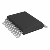
AD7328BRUZ Analog Devices Inc, AD7328BRUZ Datasheet - Page 27

AD7328BRUZ
Manufacturer Part Number
AD7328BRUZ
Description
IC ADC 12BIT+ SAR 8CHAN 20TSSOP
Manufacturer
Analog Devices Inc
Specifications of AD7328BRUZ
Data Interface
DSP, MICROWIRE™, QSPI™, Serial, SPI™
Design Resources
Using AD7328 in Appls with Single-Ended Industrial-Level Signals (CN0047)
Number Of Bits
12
Sampling Rate (per Second)
1M
Number Of Converters
1
Power Dissipation (max)
30mW
Voltage Supply Source
Dual ±
Operating Temperature
-40°C ~ 85°C
Mounting Type
Surface Mount
Package / Case
20-TSSOP (0.173", 4.40mm Width)
Resolution (bits)
13bit
Sampling Rate
1MSPS
Input Channel Type
Pseudo Differential, Single Ended
Supply Current
900µA
Digital Ic Case Style
TSSOP
No. Of Pins
20
Lead Free Status / RoHS Status
Lead free / RoHS Compliant
For Use With
EVAL-AD7328CBZ - BOARD EVALUATION FOR AD7328
Lead Free Status / Rohs Status
RoHS Compliant part
Electrostatic Device
Available stocks
Company
Part Number
Manufacturer
Quantity
Price
Part Number:
AD7328BRUZ
Manufacturer:
ADI/亚德诺
Quantity:
20 000
Company:
Part Number:
AD7328BRUZ-REEL7
Manufacturer:
ALLEGRO
Quantity:
1 200
REFERENCE
The AD7328 can operate with either the internal 2.5 V on-chip
reference or an externally applied reference. The internal reference
is selected by setting the REF bit in the control register to 1. On
power-up, the REF bit is 0, which selects the external reference for
the AD7328 conversion. Suitable reference sources for the AD7328
include AD780, AD1582, ADR431, REF193, and ADR391.
The internal reference circuitry consists of a 2.5 V band gap
reference and a reference buffer. When operating the AD7328
in internal reference mode, the 2.5 V internal reference is available
at the REFIN/OUT pin, which should be decoupled to AGND
using a 680 nF capacitor. It is recommended that the internal
reference be buffered before applying it elsewhere in the system.
The internal reference is capable of sourcing up to 90 μA.
On power-up, if the internal reference operation is required for
the ADC conversion, a write to the control register is necessary
to set the REF bit to 1. During the control register write, the con-
version result from the first initial conversion is invalid. The
reference buffer requires 500 μs to power up and charge the
680 nF decoupling capacitor during the power-up time.
The AD7328 is specified for a 2.5 V to 3 V reference range. When
a 3 V reference is selected, the ranges are ±12 V, ±6 V, ±3 V, and
0 V to +12 V. For these ranges, the V
equal to or greater than the maximum analog input range selected.
V
The AD7328 has a V
the serial interface operates. V
interface to both 3 V and 5 V processors. For example, if the
AD7328 is operated with a V
powered from a 3 V supply. This allows the AD7328 to accept
large bipolar input signals with low voltage digital processing.
TEMPERATURE INDICATOR
The AD7328 has an on-chip temperature indicator. The tem-
perature indicator can be used to provide local temperature
measurements on the AD7328. To access the temperature indicator,
the ADC should be configured in pseudo differential mode,
Mode 1 = Mode 0 = 1, which sets Channel Bits ADD2, ADD1,
DRIVE
DRIVE
feature to control the voltage at which
CC
DRIVE
of 5 V, the V
allows the ADC to easily
DD
and V
DRIVE
SS
supply must be
pin can be
Rev. B | Page 27 of 36
and ADD0 to 1. V
voltage within the specified pseudo differential input range for
the selected analog input range. When a conversion is initiated in
this configuration, the output code represents the temperature
(see Figure 46 and Figure 47). When using the temperature
indicator on the AD7328, the part should be operated at low
throughput rates, such as approximately 50 kSPS for the ±10 V
range and 30 kSPS for the ±2.5 V range. The throughput rate is
reduced for the temperature indicator mode because the AD7328
requires more acquisition time for this mode.
4420
4410
4400
4390
4380
4370
4360
4350
4340
5450
5400
5350
5300
5250
5200
5150
5100
Figure 47. ADC Output Code vs. Temperature for ±2.5 V Range
Figure 46. ADC Output Code vs. Temperature for ±10 V Range
–40
–40
–20
–20
IN
7 must be tied to AGND or to a small dc
0
0
TEMPERATURE (°C)
TEMPERATURE (°C)
±10V RANGE, INT REF
20
20
40
40
V
V
50kSPS
V
V
±2.5V RANGE
INT REFERENCE
30kSPS
CC
DD
60
CC
DD
/V
= V
/V
= V
SS
SS
DRIVE
DRIVE
= ±12V
60
= ±12V
80
AD7328
= 5V
= 5V
100
80


