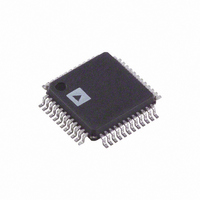
AD9975BST Analog Devices Inc, AD9975BST Datasheet - Page 18

AD9975BST
Manufacturer Part Number
AD9975BST
Description
IC FRONT-END MIXED-SGNL 48-LQFP
Manufacturer
Analog Devices Inc
Series
TxDAC+®r
Datasheet
1.AD9975BST.pdf
(20 pages)
Specifications of AD9975BST
Rohs Status
RoHS non-compliant
Number Of Bits
10
Number Of Channels
1
Voltage - Supply, Analog
3.3V
Voltage - Supply, Digital
3.3V
Package / Case
48-LQFP
Power (watts)
-
Available stocks
Company
Part Number
Manufacturer
Quantity
Price
Company:
Part Number:
AD9975BST
Manufacturer:
ADI
Quantity:
364
AD9975
Bit 7: RX LPF Tuning Update Disable
Setting this bit high disables the automatic background receive
filter calibration. The AD9975 automatically calibrates the
receive filter on reset and every few (~2) seconds thereafter to
compensate for process and temperature variation, power supply,
and long term drift. Programming a 1 to this bit disables this
function. Programming a 0 triggers an immediate first calibration
and enables the periodic update.
Register 5, Receive Filter Tuning Target
This register sets the filter tuning target as a function of F
See Register 4 description.
Register 6, RX Path Gain Adjust
The AD9975 uses a combination of a continuous time PGA
(CPGA) and a switched capacitor PGA (SPGA) for a gain range
of –6 dB to +36 dB with a resolution of 2 dB. The RX path gain
can be programmed over the serial interface by writing to the
RX path Gain Adjust Register or directly using the GAIN and
MSB aligned TX[5:1] Bits. The register default value is 0x00 for
the lowest gain setting (–6 dB). The register always reads back the
actual gain setting irrespective of which of the two programming
modes was used.
Bits [4:0]: RX PGA Gain
Table VI describes the gains and how they are achieved as a
function of the RX path adjust bits. It should be noted that the
value of these bits will read back the actual gain value to which
the PGA is set. If Bit 5 of this register is low, then the value read
back will be that set by the AGC[2:0] Pins.
Bit 5: PGA Gain Set through Register
Setting this bit high will result in the RX path gain being set by
writing to the PGA Gain Control Register. Default is zero, which
selects writing the gain through the AGC[2:0] pins in conjunction
with the RXBOOST pin.
Bit 6: RXBOOST
This bit is read-only. It reflects the level of the RXBOOST pin.
Bit 7: RXBOOST Active Low
Setting this bit high results in the value mapped to the RXBOOST
pin by the AGC inputs being inverted.
OSCIN
.
–18–
RX Path
Gain [4:0]
0x00
0x01
0x02
0x03
0x04
0x05
0x06
0x07
0x08
0x09
0x0A
0x0B
0x0C
0x0D
0x0E
0x0F
0x10
0x11
0x12*
0x13*
0x14*
0x15*
*When the wideband RX filter bit is set high, the RX path gain is limited to 30 dB.
Register 7, Transmit Path Settings
Bit 0: TX Data Input Twos Complement
Setting this bit high changes the TX path input data format to
twos complement. When this bit is low, the TX data format is
straight binary.
Bit 1: Sample TX Data on Falling TXCLKIN
If Bit 1 is set high, the TX path data will be sampled on the
falling edge of TXCLKIN. When this bit is low, the data will be
sampled on the rising edge of TXCLKIN.
Bit 4 to Bit 7: Interpolation Filter Select
Bits 4 to 7 define the interpolation filter characteristic and inter-
polation rate.
Bits 7:4;
The interpolation factor has a direct influence on the rate at
which the TX path will read the input data-words from the input
buffer. When the interpolation filter has been bypassed, the data
will be read out of the buffer at a rate of F
interpolator is configured to run in either of the 2 interpola-
tion modes, the data will be read out of the buffer at a rate of
0.5
Register 8, Receiver and Clock Output Settings
Bit 0: Rx Data Output Twos Complement
Setting this bit high changes the RX path input data format to
twos complement. When this bit is low, the RX data format is
straight binary.
The first of the two values refers to the mode when the lower RX LPF cutoff
frequency is chosen, or when the RX LPF filter is bypassed.
0x1; see TPC 1. 2
0x2; Interpolation Bypass.
0x5; see TPC 2. 2 Interpolation, BPF, Adj image.
F
OSCIN
Table VI. PGA Programming Map
L.
RX Path
Gain
–6
–4
–2
0
2
4
6
8
10
12
14
16
18
20
22
24
26
28
30/30
30/32
30/34
30/36
Interpolation, LPF.
CPGA
Gain
0
0
0
0
0
0
6
6
6
12
12
12
18
18
18
24
24
24
24/30
24/30
24/30
24/30
OSCIN
L. When the
REV. 0
SPGA
Gain
–6
–4
–2
0
2
4
0
2
4
0
2
4
0
2
4
0
2
4
6/0
6/2
6/4
6/6


