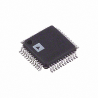
AD9975BST Analog Devices Inc, AD9975BST Datasheet - Page 13

AD9975BST
Manufacturer Part Number
AD9975BST
Description
IC FRONT-END MIXED-SGNL 48-LQFP
Manufacturer
Analog Devices Inc
Series
TxDAC+®r
Datasheet
1.AD9975BST.pdf
(20 pages)
Specifications of AD9975BST
Rohs Status
RoHS non-compliant
Number Of Bits
10
Number Of Channels
1
Voltage - Supply, Analog
3.3V
Voltage - Supply, Digital
3.3V
Package / Case
48-LQFP
Power (watts)
-
Available stocks
Company
Part Number
Manufacturer
Quantity
Price
Company:
Part Number:
AD9975BST
Manufacturer:
ADI
Quantity:
364
RECEIVE PATH DESCRIPTION
The receive path consists of a two stage PGA, a continuous
time, 4-pole LPF, an ADC, and a digital HPF. Also working
in conjunction with the receive path is an offset correction
circuit and a digital phase-locked loop. Each of these blocks
will be discussed in detail in the following sections.
PROGRAMMABLE GAIN AMPLIFIER
The PGA has a programmable gain range from –6 dB to +36 dB
if the narrower (approximately 12 MHz) LPF bandwidth is selected,
or if the LPF is bypassed. If the wider (approximately 29 MHz)
LPF bandwidth is selected, the gain range is –6 dB to +30 dB.
The PGA is comprised of two sections, a continuous time PGA
(CPGA), and a switched capacitor PGA (SPGA). The CPGA
has possible gain settings of 0, 6, 12, 18, 24 and 30. The SPGA
has possible gain settings of –6 dB, –4 dB, –2 dB, 0 dB, +2 dB,
+4 dB, and +6 dB. Table II shows how the gain is distributed
for each programmed gain setting.
The CPGA input appears at the device RX+ and RX– input pins.
The input impedance of this stage is nominally 270 Ω differential
and is not gain dependent. It is best to ac-couple the input signal
to this stage and let the inputs self-bias. This will lower the
offset voltage of the input signal, which is important at higher
gains, since any offset will lower the output compliance range of
the CPGA output. When the inputs are driven by direct coupling,
the dc level should be AVDD/2. However, this could lead to
larger dc offsets and reduce the dynamic range of the RX path.
There are two modes for selecting the RX path gain. The first
mode is to program the PGA through the serial port. A 5-bit
word determines the gain with a resolution of 2 dB per step.
More detailed information about this mode is included in the
Register Programming Definitions section of this data sheet.
The second mode sets the gain through the asynchronous
AGC[2:0] pins. These three pins set the PGA gain and state of
the RXBOOST pin according to Table II.
AGC
[2:0]
0x00
0x01
0x02
0x03
0x04
0x05
0x06
0x07
LOW-PASS FILTER
The low-pass filter (LPF) is a programmable, three-stage, fourth
order low-pass filter. The first real pole is implemented within
the CPGA. The second filter stage implements a complex pair
of poles. The last real pole is implemented in a buffer stage that
drives the SPGA.
REV. 0
Rx
Path
Gain
–6
–6
2
10
2
10
18
26
Table II. AGC[2:0] Gain Mapping
CPGA
Gain
–6
–6
–6
0
–6
0
12
18
SPGA
Gain
0
0
8
10
8
10
6
8
RXBOOST
0
0
0
0
1
1
1
1
–13–
There are two pass band settings for the LPF. Within each pass
band, the filters are tunable over about a ± 15% frequency range.
The formula for the cutoff frequency is:
Where Target is the decimal value programmed as the tuning
target in Register 5.
This filter may also be bypassed. In this case, the bandwidth of
the RX path will be gain dependent and will be around 50 MHz
at the highest gain settings.
ADC
The AD9975’s analog-to-digital converter implements pipelined
multistage architecture to achieve high sample rates while consum-
ing low power. The ADC distributes the conversion over several
smaller A/D subblocks, refining the conversion with progressively
higher accuracy as it passes the results from stage to stage. As a
consequence of the distributed conversion, ADCs require a small
fraction of the 2
type A/D. A sample-and-hold function within each of the stages
permits the first stage to operate on a new input sample while the
remaining stages operate on preceding samples. Each stage of
the pipeline, excluding the last, consists of a low resolution
Flash A/D connected to a switched capacitor DAC and interstage
residue amplifier (MDAC). The residue amplifier amplifies the
difference between the reconstructed DAC output and the flash
input for the next stage in the pipeline. One bit of redundancy is
used in each one of the stages to facilitate digital correction of
flash errors. The last stage simply consists of a Flash A/D.
AINP
AINN
The digital data outputs of the ADC are represented in straight
binary format. They saturate to full scale or zero when the input
signal exceeds the input voltage range.
The maximum value will be output from the ADC when the
RX+ input is 1 V or more greater than the RX– input. The mini-
mum value will be output from the ADC when the RX– input is
1 V or more greater than the RX+ input. This results in a full-scale
ADC voltage of 2 Vppd.
The data can be translated to straight binary data format by
simply inverting the most significant bit.
The timing of the interface is fully described in the Digital Inter-
face Port Timing section.
A/D
SHA
Figure 1. ADC Theory of Operation
n
F
D/A
comparators used in a traditional n-bit flash-
C
=
F
ADC
GAIN
×
CORRECTION LOGIC
64
/ (
A/D
64
SHA
+
Target
D/A
AD9975
)
GAIN
A/D


