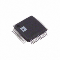
AD9975BST Analog Devices Inc, AD9975BST Datasheet - Page 14

AD9975BST
Manufacturer Part Number
AD9975BST
Description
IC FRONT-END MIXED-SGNL 48-LQFP
Manufacturer
Analog Devices Inc
Series
TxDAC+®r
Datasheet
1.AD9975BST.pdf
(20 pages)
Specifications of AD9975BST
Rohs Status
RoHS non-compliant
Number Of Bits
10
Number Of Channels
1
Voltage - Supply, Analog
3.3V
Voltage - Supply, Digital
3.3V
Package / Case
48-LQFP
Power (watts)
-
Available stocks
Company
Part Number
Manufacturer
Quantity
Price
Company:
Part Number:
AD9975BST
Manufacturer:
ADI
Quantity:
364
AD9975
DIGITAL HPF
Following the ADC, there is a bypassable digital HPF. The
response is a single pole IIR HPF. The transfer function is
approximately:
where the sampling period is equal to the ADC clock period.
This results in a 3 dB frequency approximately 1/400th of the
ADC sampling rate. The transfer function of the digital HPF with
an ADC sample rate of 50 MSPS is plotted in TPC 23.
The digital HPF introduces a 1 ADC clock cycle latency. If the
HPF function is not desired, the HPF can be bypassed and the
latency will not be incurred.
CLOCK AND OSCILLATOR CIRCUITRY
The AD9975 generates all internally required clocks from a single
clock source. This source can be supplied in one of two ways.
The first method uses the on-chip oscillator by connecting a
fundamental frequency quartz crystal between the OSC IN (Pin 1)
and XTAL (Pin 48) with parallel resonant load capacitors as
specified by the crystal manufacturer. Alternatively, a TTL-level
clock applied to OCS IN with the XTAL pin left unconnected
can overdrive the internal oscillator circuit.
The PLL has a frequency capture range between 10 MHz and
50 MHz.
AGC TIMING CONSIDERATIONS
When implementing the AGC timing loop, it is important to
consider the delay and settling time of the RX path in response
to a change in gain. Figure 2 shows the delay the receive signal
experiences through the blocks of the RX path. Whether the gain
is programmed through the serial port or via the AGC[2:0] pins,
the gain takes effect immediately with the delays shown in Figure 2.
When gain changes do not involve the CPGA, the new gain will
be evident in samples after about 7 ADC clock cycles. When the
gain change does involve the CPGA, it takes an additional 45 ns
to 70 ns due to the propagation delays of the buffer, LPF and PGA.
Table VI in the Register Programming section details the PGA
programming map.
1 CLK CYCLE
DIGITAL HPF
H z
5 CLK CYCLE 1/2 CLK CYCLE
( ) ( – .
A/D
Figure 2. AGC Loop Timing
=
Z
GAIN REGISTER
0 99994
SHA
) / ( – .
5ns
Z
BUFFER
10ns
DECODE LOGIC
0 98466
25ns OR 50ns
LPF
)
10ns
PGA
–14–
AGC PROGRAMMING
The gain in the receive path can be programmed in two ways.
The default method is through the AGC[2:0] pins. In this mode,
the gain is achieved using a combination of internal and external
gain. The external gain is controlled by the RXBOOST output
pin, which is determined by the decode of the 3-bit AGC gain value.
DIGITAL INTERFACE PORT OPERATION
The digital interface port is a 10-bit bidirectional bus shared in
burst fashion between the transmit path and receive path. The
MxFE acts as a slave to the digital ASIC, accepting two input
enable signals, TXEN and RXEN, as well as two input clock
signals, TXCLK and RXCLK. Because the sampling clocks for
the DAC and ADC are derived internally from the OSC IN
signal, it is required that the TXCLK and RXCLK signals are
exactly the same frequency as the OSC IN signal. The phase
relationships between the TXCLK, RXCLK, and OSC IN signal
are arbitrary.
In order to add flexibility to the digital interface port, there are
several programming options available. The data input format is
straight binary by default. It is possible to independently change
the data format of the transmit path and receive path to twos
complement. Also, the clock timing can be independently changed
on the transmit and receive paths by selecting either the rising
or falling clock edge as the validating/sampling edge of the clock.
The digital interface port can also be programmed into a three-
state output mode allowing it to be connected onto a shared bus.
The timing of the interface is fully described in the Digital Inter-
face Port Timing section.
CLOCK DISTRIBUTION
The DAC sampling clock, f
digital phase-locked loop (DPLL). f
L × f
the crystal oscillator when a crystal is connected between the
OSC IN and XTAL pins or by the clock that is fed into the
OSC IN pin, and L is the multiplier programmed through the
serial port. L can have the values of 1, 2, 4, or 8.
When the interpolation filter is enabled (either 2× LPF or 2× BPF
is selected), the data rate is upsampled by a factor of two. In this
case, the transmit path expects a new data input word at the rate
of f
path expects a new input word at the same frequency as DAC
sampling clock, f
frequency should be:
where K is the interpolation factor. The interpolation factor, K, is
equal to 2 when the interpolator is enabled and is equal to 1 when
the interpolator is bypassed.
The ADC sampling clock is derived from f
output sample is available every f
sampling lock can be programmed to be equal to f
The timing of the digital interface port is illustrated in the
Figures 3 and 4.
DAC
OSCIN
/2. When the interpolation filter is bypassed, the transmit
, where f
DAC
OSCIN
. Therefore, in terms of f
f
TXCLK
is the internal signal generated either by
DAC
=
L
, is generated by the internal
×
OSCIN
f
DAC
OSCIN
clock cycle. The ADC
has a frequency equal to
/
K
OSCIN
OSCIN
OSCIN
and a new
, the TXCLK
if desired.
REV. 0


