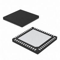
MAX19708ETM+T Maxim Integrated Products, MAX19708ETM+T Datasheet - Page 18

MAX19708ETM+T
Manufacturer Part Number
MAX19708ETM+T
Description
IC ANLG FRNT END 48-TQFN
Manufacturer
Maxim Integrated Products
Datasheet
1.MAX19708ETMT.pdf
(37 pages)
Specifications of MAX19708ETM+T
Number Of Bits
10
Number Of Channels
4
Power (watts)
36.9mW
Voltage - Supply, Analog
3V
Voltage - Supply, Digital
3V
Package / Case
48-TQFN Exposed Pad
Lead Free Status / RoHS Status
Lead free / RoHS Compliant
The dual 10-bit digital-to-analog converters (Tx DAC)
operate with clock speeds up to 11MHz. The Tx DAC
digital inputs, D0–D9, are multiplexed on a single 10-bit
bus. The voltage reference determines the Tx path full-
scale voltage at IDP, IDN and QDP, QDN analog out-
puts. See the Reference Configurations section for
setting reference voltage. Each Tx path output channel
integrates a lowpass filter tuned to meet the TD-SCDMA
spectral mask requirements.
10-Bit, 11Msps, Ultra-Low-Power
Analog Front-End
18
Figure 3. Rx ADC System Timing Diagram
Table 2. Tx Path Output Voltage vs. Input Codes
(Internal Reference Mode V
Full Scale and V
DIFFERENTIAL OUTPUT VOLTAGE (V)
CHQ
D0–D9
CLK
CHI
t
______________________________________________________________________________________
DOQ
Dual 10-Bit Tx DAC and Transmit Path
(
(
(
(
(
(
(
V
V
V
t
V
V
V
V
CL
D0Q
FS
FS
FS
FS
FS
FS
FS
FS
)
)
)
)
)
)
)
t
CLK
−
−
−
V
V
V
V
REFDAC
V
V
V
REFDAC
REFDAC
REFDAC
= 500 for 1V
1024
1024
1024
1024
REFDAC
REFDAC
REFDAC
1024
1024
1024
t
CH
D1I
×
×
×
×
×
×
×
REFDAC
t
1023
1023
1023
1023
1023
1021
DOI
1023
1023
1023
1023
1021
D1Q
3
1
1
P-P
Full Scale)
= 1.024V, External Reference Mode V
D2I
D2Q
5.5 CLOCK-CYCLE LATENCY (CHQ)
5 CLOCK-CYCLE LATENCY (CHI)
OFFSET BINARY (D0–D9)
D3I
11 1111 1111
11 1111 1110
10 0000 0001
10 0000 0000
01 1111 1111
00 0000 0001
00 0000 0000
D3Q
The TD-SCDMA filters are tuned for 1.32MHz cutoff fre-
quency and > 55dB image rejection at f
4.32MHz, f
Figure 4 for an illustration of the filter frequency response.
Buffer amplifiers follow the TD-SCDMA filters. The amplifi-
er outputs (IDN, IDP, QDN, QDP) are biased at an
adjustable common-mode DC level and designed to
drive a differential input stage with ≥ 70kΩ input imped-
ance. This simplifies the analog interface between RF
D4I
OUT
REFDAC
D4Q
= 800kHz, and f
= V
D5I
REFIN
INPUT DECIMAL CODE
D5Q
; V
FS
CLK
1023
1022
513
512
511
= 410 for 820mV
1
0
D6I
= 5.12MHz. See
D6Q
IMAGE
P-P
=


