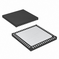
MAX19710ETN+T Maxim Integrated Products, MAX19710ETN+T Datasheet - Page 30

MAX19710ETN+T
Manufacturer Part Number
MAX19710ETN+T
Description
IC ANLG FRNT END 56-TQFN
Manufacturer
Maxim Integrated Products
Datasheet
1.MAX19710ETN.pdf
(37 pages)
Specifications of MAX19710ETN+T
Number Of Bits
10
Number Of Channels
2
Power (watts)
30mW
Voltage - Supply, Analog
3V
Voltage - Supply, Digital
3V
Package / Case
56-TQFN Exposed Pad
Lead Free Status / RoHS Status
Lead free / RoHS Compliant
10-Bit, 7.5Msps, Full-Duplex
Analog Front-End
Rx ADC inputs only requires half the signal swing com-
pared to single-ended mode. Figure 10 shows an RF
transformer converting the MAX19710 Tx DAC differen-
tial analog outputs to single-ended.
Drive the MAX19710 Rx ADC with op amps when a
balun transformer is not available. Figures 11 and 12
show the Rx ADC being driven by op amps for AC-cou-
pled single-ended and DC-coupled differential applica-
tions. Amplifiers such as the MAX4454 and MAX4354
provide high speed, high bandwidth, low noise, and
low distortion to maintain the input signal integrity. The
op-amp circuit shown in Figure 12 can also be used to
interface with the Tx DAC differential analog outputs to
provide gain or buffering. The Tx DAC differential ana-
log outputs cannot be used in single-ended mode
because of the internally generated common-mode
level. Also, the Tx DAC analog outputs are designed to
drive a differential input stage with input impedance ≥
70kΩ. If single-ended outputs are desired, use an
amplifier to provide differential-to-single-ended conver-
sion and select an amplifier with proper input common-
mode voltage range.
Figure 13 illustrates a typical FDD application circuit. The
MAX19710 interfaces directly with a ZIF radio front-end to
provide a complete “RF-to-Bits” solution for FDD applica-
tions such as private mobile radio (PMR), broadband
access radio, and proprietary radio systems. The
MAX19710 provides several system benefits to digital
baseband developers:
•
•
•
•
•
•
•
The MAX19710 requires high-speed board layout design
techniques. Refer to the MAX19710 EV kit data sheet for a
board layout reference. Place all bypass capacitors as
close to the device as possible, preferably on the same
side of the board as the device, using surface-mount
devices for minimum inductance. Bypass V
with a 0.1µF ceramic capacitor in parallel with a 2.2µF
30
30
Fast Time-to-Market
High-Performance, Low-Power Analog Functions
Low-Risk, Proven Analog Front-End Solution
No Mixed-Signal Test Times
No NRE Charges
No IP Royalty Charges
Enables Digital Baseband and Scale with 65nm to
90nm CMOS
______________________________________________________________________________________
______________________________________________________________________________________
Grounding, Bypassing, and
Using Op-Amp Coupling
Board Layout
FDD Application
DD
to GND
Figure 10. Balun Transformer-Coupled Differential-to-Single-
Ended Output Drive for Tx DAC
Figure 11. Single-Ended Drive for Rx ADC
V
V
IN
IN
100Ω
100Ω
100Ω
100Ω
MAX19710
0.1μF
0.1μF
QDP
QDN
IDP
IDN
REFN
REFN
REFP
REFP
1kΩ
1kΩ
1kΩ
1kΩ
R
50Ω
R
50Ω
0.1μF
0.1μF
ISO
ISO
22pF
22pF
22pF
22pF
R
50Ω
C
50Ω
C
R
C
C
ISO
IN
ISO
IN
IN
IN
V
V
OUT
OUT
COM
IAP
IAN
QAP
QAN
MAX19710


