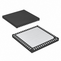
MAX19710ETN+T Maxim Integrated Products, MAX19710ETN+T Datasheet - Page 29

MAX19710ETN+T
Manufacturer Part Number
MAX19710ETN+T
Description
IC ANLG FRNT END 56-TQFN
Manufacturer
Maxim Integrated Products
Datasheet
1.MAX19710ETN.pdf
(37 pages)
Specifications of MAX19710ETN+T
Number Of Bits
10
Number Of Channels
2
Power (watts)
30mW
Voltage - Supply, Analog
3V
Voltage - Supply, Digital
3V
Package / Case
56-TQFN Exposed Pad
Lead Free Status / RoHS Status
Lead free / RoHS Compliant
DIN can be written independent of DOUT state. A 16-bit
instruction at DIN updates the device configuration. To
prevent modifying internal registers while reading data
from DOUT, hold DIN at a high state (only applies if
sequential aux-ADC conversions are not executed).
This effectively writes all ones into address 1111. Since
address 1111 does not exist, no internal registers
are affected.
Table 18. Reference Modes
Figure 9. Balun Transformer-Coupled Single-Ended-to-
Differential Input Drive for Rx ADC
V
V
1.024V ±10%
> 0.8V x V
IN
IN
V
0.1μF
0.1μF
REFIN
DD
0.33μF
0.33μF
______________________________________________________________________________________
______________________________________________________________________________________
Internal Reference Mode. V
with a 0.33µF capacitor.
Buffered External Reference Mode. An external 1.024V ±10% reference voltage is applied to REFIN. V
internally generated to be V
REFIN to GND with a 0.1µF capacitor.
25Ω
25Ω
25Ω
25Ω
0.1μF
0.1μF
22pF
22pF
22pF
22pF
IAP
COM
IAN
QAP
QAN
MAX19710
REF
REFIN
is internally generated to be 0.512V. Bypass REFP, REFN, and COM each
10-Bit, 7.5Msps, Full-Duplex
/ 2. Bypass REFP, REFN, and COM each with a 0.33µF capacitor. Bypass
REFERENCE MODE
The MAX19710 features an internal precision 1.024V-
bandgap reference that is stable over the entire power-
supply and temperature ranges. The REFIN input
provides two modes of reference operation. The volt-
age at REFIN (V
mode (Table 18).
In internal reference mode, connect REFIN to V
V
level. COM, REFP, and REFN are low-impedance out-
puts with V
and V
and COM each with a 0.33µF capacitor. Bypass REFIN
to GND with a 0.1µF capacitor.
In buffered external reference mode, apply 1.024V
±10% at REFIN. In this mode, COM, REFP, and REFN
are low-impedance outputs with V
V
V
0.33µF capacitor. Bypass REFIN to GND with a 0.1µF
capacitor. In this mode, the Tx path full-scale output is
proportional to the external reference. For example, if
the V
scale output is also increased by 10% or ±440mV.
An RF transformer (Figure 9) provides an excellent
solution to convert a single-ended signal source to a
fully differential signal for optimum ADC performance.
Connecting the center tap of the transformer to COM
provides a V
transformer can be used, or a step-up transformer can
be selected to reduce the drive requirements. In gener-
al, the MAX19710 provides better SFDR and THD with
fully differential input signals than single-ended signals,
especially for high input frequencies. In differential
mode, even-order harmonics are lower as both inputs
(IAP, IAN, QAP, QAN) are balanced, and each of the
REF
REFP
REFIN
REFIN
is an internally generated 0.512V ±4% reference
REFN
Using Balun Transformer AC-Coupling
= V
/ 4. Bypass REFP, REFN, and COM each with a
DD
COM
is increased by 10% (max), the Tx path full-
= V
DD
Analog Front-End
/ 2 + V
DD
Applications Information
= V
/ 2 DC level shift to the input. A 1:1
REFIN
/ 2 - V
DD
REFIN
Reference Configurations
) sets the reference operation
/ 2, V
REF
/ 4, and V
REFP
/ 2. Bypass REFP, REFN,
= V
DD
REFN
COM
/ 2 + V
= V
= V
DD
REF
DD
REF
/ 2 -
is
/ 2,
DD
/ 2,
29
29
.


