ISL98002CRZ-170 Intersil, ISL98002CRZ-170 Datasheet - Page 12

ISL98002CRZ-170
Manufacturer Part Number
ISL98002CRZ-170
Description
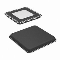
IC VID DIGITIZER 3CHN AFE 72-QFN
Manufacturer
Intersil
Datasheet
1.ISL98002CRZ-140.pdf
(28 pages)
Specifications of ISL98002CRZ-170
Number Of Bits
8
Number Of Channels
3
Power (watts)
535mW
Voltage - Supply, Analog
3 V ~ 3.6 V
Voltage - Supply, Digital
3 V ~ 3.6 V
Package / Case
72-VFQFN Exposed Pad
Lead Free Status / RoHS Status
Lead free / RoHS Compliant
Register Listing
ADDRESS
0x0A
0x0B
0x0C
0x0D
0x0E
0x0F
0x09
0x10
0x11
0x12
Red Offset (0x80)
Green Offset (0x80)
Blue Offset (0x80)
Offset DAC Configuration (0x00)
AFE Bandwidth (0x2E)
PLL Htotal MSB (0x03)
PLL Htotal LSB (0x20)
PLL Sampling Phase (0x00)
PLL Pre-coast (0x04)
PLL Post-coast (0x04)
REGISTER (DEFAULT VALUE)
(Continued)
12
BIT(S)
7:0
7:0
7:0
3:2
5:4
7:6
3:1
7:4
5:0
7:0
5:0
7:0
7:0
0
1
0
ISL98002
Blue Offset
Pre-coast
Red Offset
Green Offset
Offset DAC Range
Reserved
Red Offset DAC
LSBs
Green Offset DAC
LSBs
Blue Offset DAC
LSBs
Unused
AFE BW
Peaking
PLL Htotal MSB
PLL Htotal LSB
PLL Sampling Phase Used to control the phase of the ADC’s sample point
Post-coast
FUNCTION NAME
ABLC™ enabled: digital offset control. A 1 LSB
change in this register will shift the ADC output by
1 LSB. ABLC™ disabled: analog offset control. These
bits go to the upper 8-bits of the 10-bit offset DAC. A
1 LSB change in this register will shift the ADC output
approximately 1 LSB (Offset DAC range = 0) or
0.5LSBs (Offset DAC range = 1).
0x00 = min DAC value or -0x80 digital offset,
0x80 = mid DAC value or 0x00 digital offset,
0xFF = max DAC value or +0x7F digital offset
0: ±½ ADC full-scale (1 DAC LSB ~ 1 ADC LSB)
1: ±¼ ADC full-scale (1 DAC LSB ~ ½ ADC LSB)
Set to 0.
These bits are the LSBs necessary for 10-bit manual
offset DAC control.
Combine with their respective MSBs in registers
0x09, 0x0A, and 0x0B to achieve 10-bit offset DAC
control.
Value doesn’t matter
3dB point for AFE lowpass filter
000b: 100MHz
111b: 780MHz (default)
0x0: Peaking off
0x1: Moderate peaking
0x2: Maximum recommended peaking (default)
Values above 2 are not recommended.
14-bit HTOTAL (number of active pixels) value
The minimum HTOTAL value supported is 0x200.
HTOTAL to PLL is updated on LSB write only.
relative to the period of a pixel. Adjust to obtain
optimum image quality. One step = 5.625° (1.56% of
pixel period).
Number of lines the PLL will coast prior to the start of
VSYNC.
Number of lines the PLL will coast after the end of
VSYNC.
DESCRIPTION
March 26, 2008
FN6535.0


