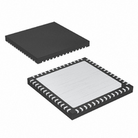
MAX19713ETN+ Maxim Integrated Products, MAX19713ETN+ Datasheet - Page 24

MAX19713ETN+
Manufacturer Part Number
MAX19713ETN+
Description
IC ANLG FRONT END 45MSPS 56-TQFN
Manufacturer
Maxim Integrated Products
Datasheet
1.MAX19713ETN.pdf
(37 pages)
Specifications of MAX19713ETN+
Number Of Bits
10
Number Of Channels
2
Power (watts)
91.8mW
Voltage - Supply, Analog
3V
Voltage - Supply, Digital
3V
Package / Case
56-TQFN Exposed Pad
Lead Free Status / RoHS Status
Lead free / RoHS Compliant
10-Bit, 45Msps, Full-Duplex
Analog Front-End
the on-board converters are already powered.
Consequently, power consumption in this mode is the
maximum of all operating modes. In FD mode the
MAX19713 consumes 91.8mW.
The MAX19713 uses the SPI interface to control the
operating modes of the device including the shutdown
and wake-up functions. Once the device has been
placed in shutdown through the appropriate SPI com-
mand, the first pulse on CS/WAKE performs a wake-up
function. At the first rising edge of CS/WAKE, the
MAX19713 is forced to a preset operating mode deter-
mined by the WAKEUP-SEL register. This mode is
Table 9. Offset Control Bits for ID and QD Channels (IOFFSET or QOFFSET Mode)
Note: 1 LSB = (800mV
24
Table 10. Common-Mode Select
(COMSEL Mode)
CM1
0
0
1
1
IO5/QO5
______________________________________________________________________________________
1
1
1
1
1
1
0
0
0
0
0
0
•
•
•
•
•
•
BITS IO5–IO0 WHEN IN IOFFSET MODE, BITS QO5–QO0 WHEN IN QOFFSET MODE
CM0
0
1
0
1
Tx PATH OUTPUT COMMON MODE (V)
P-P
IO4/QO4
/ 1023) = 0.782mV.
1
1
1
0
0
0
0
0
0
1
1
1
•
•
•
•
•
•
1.06 (Default)
0.94
0.82
0.71
Wake-Up Function
IO3/QO3
1
1
1
0
0
0
0
0
0
1
1
1
•
•
•
•
•
•
IO2/QO2
1
1
1
0
0
0
0
0
0
1
1
1
•
•
•
•
•
•
termed the wake-up state. If the WAKEUP-SEL register
has not been programmed, the wake-up state for the
MAX19713 is FD mode by default (Tables 6, 11). The
WAKEUP-SEL register cannot be programmed with W2
= 0, W1 = 0, and W0 = 0. If this value is inadvertently
written to the device, it is ignored and the register con-
tinues to store its previous value. Upon wake-up, the
Table 11. WAKEUP-SEL Register
W2
0
0
0
0
1
1
1
1
IO1/QO1
W1
0
0
1
1
0
0
1
1
1
1
0
1
0
0
0
0
1
0
1
1
•
•
•
•
•
•
W0
0
1
0
1
0
1
0
1
Invalid Value. This value is ignored
POWER MODE AFTER WAKE-UP
when inadvertently written to the
IO0/QO0
1
0
1
0
1
0
0
1
0
1
0
1
WAKEUP-SEL register.
•
•
•
•
•
•
(WAKE-UP STATE)
SPI1-SLOW Rx
SPI2-SLOW Tx
SPI3-FAST Rx
SPI4-FAST Tx
FD (Default)
STBY
IDLE
OFFSET 1 LSB =
(VFS
0mV (Default)
-31 LSB
-30 LSB
-29 LSB
29 LSB
30 LSB
31 LSB
-2 LSB
-1 LSB
P-P
1 LSB
2 LSB
0mV
•
•
•
•
•
•
/ 1023)


