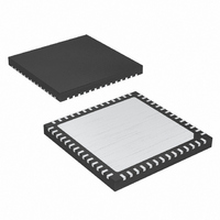
MAX19713ETN+ Maxim Integrated Products, MAX19713ETN+ Datasheet - Page 16

MAX19713ETN+
Manufacturer Part Number
MAX19713ETN+
Description
IC ANLG FRONT END 45MSPS 56-TQFN
Manufacturer
Maxim Integrated Products
Datasheet
1.MAX19713ETN.pdf
(37 pages)
Specifications of MAX19713ETN+
Number Of Bits
10
Number Of Channels
2
Power (watts)
91.8mW
Voltage - Supply, Analog
3V
Voltage - Supply, Digital
3V
Package / Case
56-TQFN Exposed Pad
Lead Free Status / RoHS Status
Lead free / RoHS Compliant
10-Bit, 45Msps, Full-Duplex
Analog Front-End
The MAX19713 integrates three 12-bit auxiliary DACs
(aux-DACs) and a 10-bit, 333ksps auxiliary ADC (aux-
ADC) with 4:1 input multiplexer. The aux-DAC channels
feature 1µs settling time for fast AGC, VGA, and AFC
level setting. The aux-ADC features data averaging to
reduce processor overhead and a selectable clock-
divider to program the conversion rate.
The MAX19713 includes a 3-wire serial interface to con-
trol operating modes and power management. The seri-
al interface is SPI™ and MICROWIRE™ compatible.
The MAX19713 serial interface selects shutdown, idle,
standby, FD, transmit (Tx), and receive (Rx) modes, as
well as controls aux-DAC and aux-ADC channels.
The MAX19713 features two independent, high-speed,
10-bit buses for the Rx ADC and Tx DAC, which allow
full-duplex (FD) operation for frequency-division duplex
applications. Each bus can be disabled to optimize
power management through the 3-wire interface. The
SPI is a trademark of Motorola, Inc.
MICROWIRE is a trademark of National Semiconductor Corp.
Figure 1. Rx ADC Internal T/H Circuits
16
______________________________________________________________________________________
QAN
QAP
IAN
IAP
S4a
S4b
S4a
S4b
S4c
S4c
C2a
C2b
C2a
C2b
INTERNAL
S2a
INTERNAL
INTERNAL
S2a
INTERNAL
BIAS
BIAS
BIAS
BIAS
S1
S1
S2b
S2b
C1a
C1b
C1a
C1b
COM
COM
COM
COM
S5a
S5b
S5a
S5b
S3a
S3b
S3a
S3b
MAX19713 operates from a single 2.7V to 3.3V analog
supply and a 1.8V to 3.3V digital supply.
The ADC uses a seven-stage, fully differential, pipelined
architecture that allows for high-speed conversion while
minimizing power consumption. Samples taken at the
inputs move progressively through the pipeline stages
every half clock cycle. Including the delay through the
output latch, the total clock-cycle latency is 5 clock
cycles for channel IA and 5.5 clock cycles for channel
QA. The ADC full-scale analog input range is ±V
with a V
is the difference between V
Reference Configurations section for details.
Figure 1 displays a simplified diagram of the Rx ADC
input track-and-hold (T/H) circuitry. Both ADC inputs
(IAP, QAP, IAN, and QAN) can be driven either differen-
tially or single-ended. Match the impedance of IAP and
OUT
OUT
OUT
OUT
HOLD
TRACK
DD
MAX19713
HOLD
/ 2 (±0.8V) common-mode input range. V
TRACK
CLK
INTERNAL
NONOVERLAPPING
CLOCK SIGNALS
Input Track-and-Hold (T/H) Circuits
REFP
Dual 10-Bit Rx ADC
and V
REFN
. See the
REF
REF


