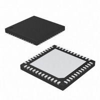
MAX19707ETM+ Maxim Integrated Products, MAX19707ETM+ Datasheet - Page 9

MAX19707ETM+
Manufacturer Part Number
MAX19707ETM+
Description
IC ANLG FRONT END 45MSPS 48-TQFN
Manufacturer
Maxim Integrated Products
Datasheet
1.MAX19707ETM.pdf
(37 pages)
Specifications of MAX19707ETM+
Number Of Bits
10
Number Of Channels
4
Power (watts)
84.6mW
Voltage - Supply, Analog
3V
Voltage - Supply, Digital
3V
Package / Case
48-TQFN Exposed Pad
Lead Free Status / RoHS Status
Lead free / RoHS Compliant
ELECTRICAL CHARACTERISTICS (continued)
(V
amplitude = -0.5dBFS, Tx DAC output amplitude = 0dBFS, differential Rx ADC input, differential Tx DAC output, C
C
Note 1: Specifications from T
Note 2: The minimum clock frequency (f
Note 3: SNR, SINAD, SFDR, HD3, and THD are based on a differential analog input voltage of -0.5dBFS referenced to the amplitude
Note 4: Crosstalk rejection is measured by applying a high-frequency test tone to one channel and a low-frequency tone to the second
Note 5: Amplitude and phase matching is measured by applying the same signal to each channel, and comparing the two output
Note 6: Guaranteed by design and characterization.
SPI is a trademark of Motorola, Inc.
DIGITAL INPUTS (CLK, SCLK, DIN, CS, D0–D9, T/R, SHDN)
Input High Threshold
Input Low Threshold
Input Leakage
Input Capacitance
DIGITAL OUTPUTS (D0–D9, DOUT)
Output-Voltage Low
Output-Voltage High
Tri-State Leakage Current
Tri-State Output Capacitance
COM
DD
= 3V, OV
= 0.33µF, unless otherwise noted. C
guaranteed by design and characterization.
quency (ACLK) is determined by f
7.5MHz / 128 = 58.6kHz. The aux-ADC conversion time does not include the time to clock the serial data out of the SPI™.
The maximum conversion time (for no averaging, NAVG = 1) will be, t
of the digital outputs. SINAD and THD are calculated using HD2 through HD6.
channel. FFTs are performed on each channel. The parameter is specified as the power ratio of the first and second channel
FFT test tone.
signals using a sine-wave fit.
PARAMETER
DD
= 1.8V, internal reference (1.024V), C
_______________________________________________________________________________________
A
= +25°C to +85°C are guaranteed by production tests. Specifications from T
SYMBOL
CLK
I
C
DC
V
V
DI
V
LEAK
V
10-Bit, 45Msps, Ultra-Low-Power
L
OUT
INH
INL
CLK
OH
OL
IN
< 5pF on all aux-DAC outputs. Typical values are at T
IN
) for the MAX19707 is 7.5MHz (typical). The minimum aux-ADC sample rate clock fre-
and the chosen aux-ADC clock-divider value. The minimum aux-ADC ACLK >
D0–D9, CLK, SCLK, DIN, CS, T/R,
SHDN = OGND or OV
I
I
SINK
SOURCE
L
≈ 10pF on all digital outputs, f
= 200µA
= 200µA
CONDITIONS
DD
CONV
(max) = (12 x 1 x 128) / 7.5MHz = 205µs.
Analog Front-End
CLK
= 45MHz (50% duty cycle), Rx ADC input
0.7 x OV
0.8 x OV
A
MIN
-1
-1
= +25°C.) (Note 1)
DD
DD
TYP
A
5
5
= +25°C to -40°C are
0.3 x OV
0.2 x OV
MAX
REFP
+1
+1
DD
DD
= C
UNITS
REFN
µA
pF
µA
pF
V
V
V
V
9
=


