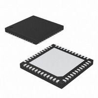
MAX19707ETM+ Maxim Integrated Products, MAX19707ETM+ Datasheet - Page 15

MAX19707ETM+
Manufacturer Part Number
MAX19707ETM+
Description
IC ANLG FRONT END 45MSPS 48-TQFN
Manufacturer
Maxim Integrated Products
Datasheet
1.MAX19707ETM.pdf
(37 pages)
Specifications of MAX19707ETM+
Number Of Bits
10
Number Of Channels
4
Power (watts)
84.6mW
Voltage - Supply, Analog
3V
Voltage - Supply, Digital
3V
Package / Case
48-TQFN Exposed Pad
Lead Free Status / RoHS Status
Lead free / RoHS Compliant
The MAX19707 integrates a dual, 10-bit Rx ADC and a
dual, 10-bit Tx DAC while providing ultra-low power
and high dynamic performance at a 45Msps conver-
sion rate. The Rx ADC analog input amplifiers are fully
differential and accept 1.024V
Tx DAC analog outputs are fully differential with
±400mV full-scale output, selectable common-mode
DC level, and adjustable I/Q offset trim.
The MAX19707 integrates three 12-bit auxiliary DAC
(aux-DAC) channels and a 10-bit, 333ksps auxiliary
ADC (aux-ADC) with 4:1 input multiplexer. The aux-DAC
channels feature 1µs settling time for fast automatic
gain-control (AGC), variable-gain amplifier (VGA), and
13–18, 21–24
40, 41
44, 45
PIN
10
19
20
25
26
27
28
29
30
34
35
36
37
38
46
47
48
—
QDN, QDP
IDN, IDP
D0–D9
OGND
______________________________________________________________________________________
NAME
SHDN
DOUT
REFIN
OV
ADC2
ADC1
DAC3
DAC2
DAC1
SCLK
REFN
COM
QAP
DIN
T/R
CS
EP
DD
Detailed Description
Channel-QA Positive Analog Input. For single-ended operation, connect signal source to QAP.
Digital I/O. Outputs for receive ADC in Rx mode. Inputs for transmit DAC in Tx mode. D9 is the most
significant bit (MSB) and D0 is the least significant bit (LSB).
Output-Driver Ground
Output-Driver Power Supply. Supply range from 1.8V to V
combination of a 2.2µF capacitor in parallel with a 0.1µF capacitor.
Active-Low Shutdown Input. Apply logic-low to place the MAX19707 in shutdown.
Aux-ADC Digital Output
Transmit- or Receive-Mode Select Input. T/R logic-low input sets the device in receive mode. A
logic-high input sets the device in transmit mode.
3-Wire Serial-Interface Data Input. Data is latched on the rising edge of the SCLK.
3-Wire Serial-Interface Clock Input
3-Wire Serial-Interface Chip-Select Input. Logic-low enables the serial interface.
Analog Input for Auxiliary ADC
Analog Input for Auxiliary ADC
Analog Output for Auxiliary DAC3
Analog Output for Auxiliary DAC2
Analog Output for Auxiliary DAC1 (AFC DAC, V
DAC Channel-ID Differential Voltage Output
DAC Channel-QD Differential Voltage Output
Reference Input. Connect to V
Common-Mode Voltage I/O. Bypass COM to GND with a 0.33µF capacitor.
Negative Reference I/O. Rx ADC conversion range is ±(V
0.33µF capacitor.
Exposed Paddle. Exposed paddle is internally connected to GND. Connect EP to the GND plane.
P-P
full-scale signals. The
10-Bit, 45Msps, Ultra-Low-Power
DD
for internal reference. Bypass to GND with a 0.1µF capacitor.
automatic frequency-control (AFC) level setting. The
aux-ADC features data averaging to reduce processor
overhead and a selectable clock-divider to program the
conversion rate.
The MAX19707 includes a 3-wire serial interface to
control operating modes and power management. The
serial interface is SPI and MICROWIRE™ compatible.
The MAX19707 serial interface selects shutdown, idle,
standby, transmit (Tx), and receive (Rx) modes, as well
as controls aux-DAC and aux-ADC channels.
The Rx ADC and Tx DAC share a common digital I/O to
reduce the digital interface to a single, 10-bit parallel
multiplexed bus. The 10-bit digital bus operates on a
single 1.8V to 3.3V supply.
MICROWIRE is a trademark of National Semiconductor Corp.
FUNCTION
OUT
Pin Description (continued)
= 1.1V During Power-Up)
Analog Front-End
REFP
DD
. Bypass OV
- V
REFN
). Bypass REFN to GND with a
DD
to OGND with a
15


