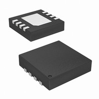
ISL1208IRT8Z-TK Intersil, ISL1208IRT8Z-TK Datasheet - Page 17

ISL1208IRT8Z-TK
Manufacturer Part Number
ISL1208IRT8Z-TK
Description
IC RTC/CALENDER I2C 8-TDFN
Manufacturer
Intersil
Type
Clock/Calendar/NVSRAMr
Datasheet
1.ISL1208IB8Z-TK.pdf
(24 pages)
Specifications of ISL1208IRT8Z-TK
Memory Size
2B
Time Format
HH:MM:SS (12/24 hr)
Date Format
YY-MM-DD-dd
Interface
I²C, 2-Wire Serial
Voltage - Supply
2.7 V ~ 5.5 V
Operating Temperature
-40°C ~ 85°C
Mounting Type
Surface Mount
Package / Case
8-TDFN
Lead Free Status / RoHS Status
Lead free / RoHS Compliant
Available stocks
Company
Part Number
Manufacturer
Quantity
Price
Company:
Part Number:
ISL1208IRT8Z-TK
Manufacturer:
Intersil
Quantity:
1 000
Device Addressing
Following a start condition, the master must output a Slave
Address Byte. The 7 MSBs are the device identifier. These
bits are “1101111”. Slave bits “1101” access the register.
Slave bits “111” specify the device select bits.
The last bit of the Slave Address Byte defines a read or write
operation to be performed. When this R/W bit is a “1”, then a
read operation is selected. A “0” selects a write operation
(Refer to Figure 15).
After loading the entire Slave Address Byte from the SDA
bus, the ISL1208 compares the device identifier and device
select bits with “1101111”. Upon a correct compare, the
device outputs an acknowledge on the SDA line.
Following the Slave Byte is a one byte word address. The
word address is either supplied by the master device or
obtained from an internal counter. On power-up the internal
address counter is set to address 0h, so a current address
read of the CCR array starts at address 0h. When required,
as part of a random read, the master must supply the 1 Word
Address Bytes as shown in Figure 16.
In a random read operation, the slave byte in the “dummy
write” portion must match the slave byte in the “read”
section. For a random read of the Clock/Control Registers,
the slave byte must be “1101111x” in both places.
FIGURE 15. SLAVE ADDRESS, WORD ADDRESS, AND DATA
A7
D7
1
FROM THE
SIGNALS
MASTER
SIGNALS FROM
SIGNAL AT
A6
D6
1
THE SLAVE
SDA
A5
D5
0
BYTES
S
A
R
T
T
A4
D4
1
1
IDENTIFICATION
1
BYTE WITH
A3
D3
0
1
R/W = 0
1 1 1 1
17
1
A2
D2
0
1
A1
D1
A
C
K
R/W
A0
D0
ADDRESS
BYTE
SLAVE
ADDRESS BYTE
WORD ADDRESS
DATA BYTE
FIGURE 16. READ SEQUENCE
A
C
K
S
A
R
T
T
ISL1208
IDENTIFICATION
1
BYTE WITH
1
R/W = 1
0
1 1 1 1
Write Operation
A Write operation requires a START condition, followed by a
valid Identification Byte, a valid Address Byte, a Data Byte,
and a STOP condition. After each of the three bytes, the
ISL1208 responds with an ACK. At this time, the I
interface enters a standby state.
Read Operation
A Read operation consists of a three byte instruction
followed by one or more Data Bytes (See Figure 16). The
master initiates the operation issuing the following
sequence: a START, the Identification byte with the R/W bit
set to “0”, an Address Byte, a second START, and a second
Identification byte with the R/W bit set to “1”. After each of
the three bytes, the ISL1208 responds with an ACK. Then
the ISL1208 transmits Data Bytes as long as the master
responds with an ACK during the SCL cycle following the
eighth bit of each byte. The master terminates the read
operation (issuing a STOP condition) following the last bit of
the last Data Byte (See Figure 16).
The Data Bytes are from the memory location indicated by
an internal pointer. This pointer initial value is determined by
the Address Byte in the Read operation instruction, and
increments by one during transmission of each Data Byte.
After reaching the memory location 13h the pointer “rolls
over” to 00h, and the device continues to output data for
each ACK received.
1
A
C
K
FIRST READ
DATA BYTE
A
C
K
A
C
K
LAST READ
DATA BYTE
September 12, 2008
2
C
FN8085.8
S
O
P
T


