CDP68HC68T1M2 Intersil, CDP68HC68T1M2 Datasheet - Page 4
CDP68HC68T1M2
Manufacturer Part Number
CDP68HC68T1M2
Description
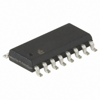
IC RTC 32X8 NVSRAM CMOS 16-SOIC
Manufacturer
Intersil
Type
Clock/Calendar/NVSRAMr
Datasheet
1.CDP68HC68T1EZ.pdf
(23 pages)
Specifications of CDP68HC68T1M2
Memory Size
32B
Time Format
HH:MM:SS (12/24 hr)
Date Format
YY-MM-DD-dd
Interface
SPI, 3-Wire Serial
Voltage - Supply
3 V ~ 6 V
Operating Temperature
-40°C ~ 85°C
Mounting Type
Surface Mount
Package / Case
16-SOIC (0.300", 7.5mm Width)
Digital Ic Case Style
SOIC
No. Of Pins
16
Operating Temperature Range
-40°C To +85°C
Peak Reflow Compatible (260 C)
No
Current Rating
12A
Leaded Process Compatible
No
Rohs Compliant
No
Bus Type
Serial (3-Wire, SPI)
Operating Supply Voltage (typ)
3.3/5V
Package Type
SOIC W
Operating Supply Voltage (max)
6V
Operating Supply Voltage (min)
3V
Operating Temperature Classification
Industrial
Operating Temperature (max)
85C
Operating Temperature (min)
-40C
Pin Count
16
Mounting
Surface Mount
Lead Free Status / RoHS Status
Contains lead / RoHS non-compliant
Available stocks
Company
Part Number
Manufacturer
Quantity
Price

Company:
Part Number:
CDP68HC68T1M2Z
Manufacturer:
Intersil
Quantity:
1 716
Part Number:
CDP68HC68T1M2Z
Manufacturer:
INTERSIL
Quantity:
20 000


Static Electrical Specifications
NOTES:
Dynamic Electrical Specifications
Operating Current (Note 3)
V
Crystal Operation
Standby Current (Note 3)
V
Crystal Operation
Input Capacitance
Maximum Rise and Fall Times
(Except XTAL Input and POR Pin 10)
Input Voltage (Line Input Pin Only, Power Sense
Mode)
V
(For V
Power-On Reset (POR) Pulse Width
2. Typical values are for T
3. Clock out (Pin 1) disabled, outputs open circuited. No serial access cycles.
IDENTIFICATION
DD
B
SYS
= 2.2V
= 5V, V
NUMBER
> V
B
Not Internally Connected to V
11
12
A
B
C
1
2
3
4
5
7
8
B
V
B
T
= 3V
PARAMETER
Chip Enable Setup Time
Chip Enable After Clock Hold Time
Clock Width High
Clock Width Low
Data In to Clock Setup Time
Clock to Data Propagation Delay
Chip Disable to Output High Z
Output Rise Time
Output Fall Time
Data in After Clock Hold Time
Clock to Data Out Active
Clock Recovery Time
A
= +25°C and nominal V
4
PARAMETER
DD
)
At T
A
Bus Timing V
= -40°C to +85°C, V
SYMBOL
DD
C
t
r
.
I
, t
B
IN
f
CDP68HC68T1
DD
t
t
t
t
t
t
t
t
t
t
t
t
EVCV
CVEX
WH
WL
DVCV
CVDV
EXQZ
r
f
CVDX
CVQX
REC
SYMBOL
32kHz
1MHz
2MHz
4MHz
32kHz
V
±10%, V
IN
= 0, T
TEST CONDITIONS
DD
= V
SS
A
= +25°C
BATT
= 0V
MIN
200
250
400
400
200
200
200
DC
= 5V ±5%, Unless Otherwise Specified. (Continued)
-
-
-
-
-
, T
V
DD
A
= -40°C to +85°C
= 3.3V
LIMITS (ALL TYPES)
MAX
200
200
200
200
200
-
-
-
-
-
-
-
MIN
100
0
-
-
-
-
-
-
-
-
0.025
0.08
0.15
CDP68HC68T1
0.3
I
D
(Note 2)
MIN
100
125
200
200
100
100
200
-
-
-
-
-
TYP
1.0
10
10
75
-
-
-
V
0.015
DD
0.15
0.25
0.4
I
B
= 5V
MAX
100
100
100
100
100
-
-
-
-
-
-
-
MAX
12
2
2
-
-
-
-
-
-
-
-
-
October 29, 2007
UNITS
UNITS
FN1547.8
ns
ns
ns
ns
ns
ns
ns
ns
ns
ns
ns
ns
mA
mA
mA
mA
mA
µA
pF
µs
µs
ns
V
V
Related parts for CDP68HC68T1M2
Image
Part Number
Description
Manufacturer
Datasheet
Request
R

Part Number:
Description:
Intersil Corporation [CMOS Serial Controller Interface]
Manufacturer:
Intersil Corporation
Datasheet:
Part Number:
Description:
Manufacturer:
Intersil Corporation
Datasheet:
Part Number:
Description:
357-036-542-201 CARDEDGE 36POS DL .156 BLK LOPRO
Manufacturer:
Intersil Corporation
Datasheet:
Part Number:
Description:
1024-Word x 4-Bit LSI Static RAM
Manufacturer:
Intersil Corporation
Datasheet:
Part Number:
Description:
General Purpose NPN Transistor Arrays FN341.4
Manufacturer:
Intersil Corporation
Datasheet:
Part Number:
Description:
CMOS 16-Bit Microprocessor
Manufacturer:
Intersil Corporation
Datasheet:
Part Number:
Description:
Manufacturer:
Intersil Corporation
Datasheet:
Part Number:
Description:
Manufacturer:
Intersil Corporation
Datasheet:
Part Number:
Description:
Manufacturer:
Intersil Corporation
Datasheet:
Part Number:
Description:
Manufacturer:
Intersil Corporation
Datasheet:
Part Number:
Description:
CMOS 6-Bit Latch and Decoder Memory Interfaces
Manufacturer:
Intersil Corporation
Datasheet:
Part Number:
Description:
CA3046General Purpose NPN Transistor Arrays
Manufacturer:
Intersil Corporation
Datasheet:
Part Number:
Description:
Manufacturer:
Intersil Corporation
Datasheet:
Part Number:
Description:
TR909 DLC/FLC SLIC with Low Power Standby
Manufacturer:
Intersil Corporation
Datasheet:
Part Number:
Description:
Manufacturer:
Intersil Corporation
Datasheet: