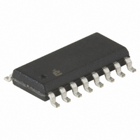
CDP68HC68T1M2 Intersil, CDP68HC68T1M2 Datasheet - Page 18

CDP68HC68T1M2
Manufacturer Part Number
CDP68HC68T1M2
Description
IC RTC 32X8 NVSRAM CMOS 16-SOIC
Manufacturer
Intersil
Type
Clock/Calendar/NVSRAMr
Datasheet
1.CDP68HC68T1EZ.pdf
(23 pages)
Specifications of CDP68HC68T1M2
Memory Size
32B
Time Format
HH:MM:SS (12/24 hr)
Date Format
YY-MM-DD-dd
Interface
SPI, 3-Wire Serial
Voltage - Supply
3 V ~ 6 V
Operating Temperature
-40°C ~ 85°C
Mounting Type
Surface Mount
Package / Case
16-SOIC (0.300", 7.5mm Width)
Digital Ic Case Style
SOIC
No. Of Pins
16
Operating Temperature Range
-40°C To +85°C
Peak Reflow Compatible (260 C)
No
Current Rating
12A
Leaded Process Compatible
No
Rohs Compliant
No
Bus Type
Serial (3-Wire, SPI)
Operating Supply Voltage (typ)
3.3/5V
Package Type
SOIC W
Operating Supply Voltage (max)
6V
Operating Supply Voltage (min)
3V
Operating Temperature Classification
Industrial
Operating Temperature (max)
85C
Operating Temperature (min)
-40C
Pin Count
16
Mounting
Surface Mount
Lead Free Status / RoHS Status
Contains lead / RoHS non-compliant
Available stocks
Company
Part Number
Manufacturer
Quantity
Price
Company:
Part Number:
CDP68HC68T1M2Z
Manufacturer:
Intersil
Quantity:
1 716
Part Number:
CDP68HC68T1M2Z
Manufacturer:
INTERSIL
Quantity:
20 000
System Diagrams
NOTE: Example of a system in which the power is controlled by an external source. The LINE input pin can sense when the switch opens by use
of the POWER-SENSE INTERRUPT. The CDP68HC68T1 crystal drives the clock input to the CPU using the CLK OUT pin. On power down when
V
always supplies power to the oscillator, keeping voltage frequency variation to a minimum.
A Procedure for Power-Down Operation might consist of the following:
1. Set power sense operation by writing Bit 5 high in the Interrupt Control Register.
2. When an interrupt occurs, the CPU reads the Status Register to determine the interrupt source.
3. Sensing a power failure, the CPU does the necessary housekeeping to prepare for shutdown.
4. The CPU reads the Status Register again after several milliseconds to determine validity of power failure.
5. The CPU sets power-down Bit 6 and disables all interrupts in the Interrupt Control Register when power down is verified.
6. When power returns and V
SYS
This causes the CPU reset and clock out to be held low and disconnects the serial interface.
communication is established.
< V
BATT
+ 1.0V. V
LINE
BATT
AC
18
will power the CDP68HC68T1. A threshold detect activates a P-Channel switch, connecting V
(Continued)
FIGURE 17. EXTERNALLY CONTROLLED POWER SYSTEM DIAGRAM
SYS
rises above V
GENERATOR
BRIDGE
V
BATT
DD
CDP68HC68T1
, power-down is terminated. The CPU reset is released and serial
V
CDP68HC68T1
LINE
BATT
CLK OUT
CPUR
MISO
MOSI
V
POR
SCK
V
SYS
INT
CE
DD
V
DD
IRQ
RESET
OSC 1
PORT (e.g., PCO)
MISO
MOSI
SCK
CDP68HC05C8B
V
DD
BATT
to V
DD
October 29, 2007
. V
BATT
FN1547.8


