ISL1219IUZ Intersil, ISL1219IUZ Datasheet - Page 4
ISL1219IUZ
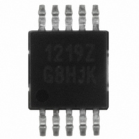
Manufacturer Part Number
ISL1219IUZ
Description
IC RTC LP BATT BACK SRAM 10MSOP
Manufacturer
Intersil
Type
Clock/Calendar/NVSRAMr
Specifications of ISL1219IUZ
Memory Size
2B
Time Format
HH:MM:SS (12/24 hr)
Date Format
YY-MM-DD-dd
Interface
I²C, 2-Wire Serial
Voltage - Supply
2.7 V ~ 5.5 V
Operating Temperature
-40°C ~ 85°C
Mounting Type
Surface Mount
Package / Case
10-MSOP, Micro10™, 10-uMAX, 10-uSOP
Clock Format
HH
Clock Ic Type
RTC
Interface Type
I2C, Serial
Memory Configuration
2 X 8
Supply Voltage Range
2.7V To 5.5V
Digital Ic Case Style
MSOP
Rohs Compliant
Yes
Lead Free Status / RoHS Status
Lead free / RoHS Compliant
Available stocks
Company
Part Number
Manufacturer
Quantity
Price
Company:

Part Number:
ISL1219IUZ
Manufacturer:
Intersil
Quantity:
490
Company:
Part Number:
ISL1219IUZ
Manufacturer:
Intersil
Quantity:
222
Part Number:
ISL1219IUZ-T
Manufacturer:
INTERSIL
Quantity:
20 000


I
2
V
V
Hysteresis SDA and SCL Input Buffer Hysteresis
V
Cpin
f
t
t
t
t
t
t
t
t
t
t
t
t
t
t
Cb
SYMBOL
SCL
IN
AA
BUF
LOW
HIGH
SU:STA
HD:STA
SU:DAT
HD:DAT
SU:STO
HD:STO
DH
R
F
C Interface Specifications
IL
IH
OL
SDA and SCL Input Buffer LOW
Voltage
SDA and SCL Input Buffer HIGH
Voltage
SDA Output Buffer LOW Voltage,
Sinking 3mA
SDA and SCL Pin Capacitance
SCL Frequency
Pulse Width Suppression Time at
SDA and SCL Inputs
SCL Falling Edge to SDA Output Data
Valid
Time the Bus Must be Free before the
Start of a New Transmission
Clock LOW Time
Clock HIGH Time
START Condition Setup Time
START Condition Hold Time
Input Data Setup Time
Input Data Hold Time
STOP Condition Setup Time
STOP Condition Hold Time
Output Data Hold Time
SDA and SCL Rise Time
SDA and SCL Fall Time
Capacitive Loading of SDA or SCL
PARAMETER
4
Test Conditions: V
V
T
V
Any pulse narrower than the
max spec is suppressed.
SCL falling edge crossing 30%
of V
to 70% of V
SDA crossing 70% of V
during a STOP condition, to
SDA crossing 70% of V
during the following START
condition.
Measured at the 30% of V
crossing.
Measured at the 70% of V
crossing.
SCL rising edge to SDA falling
edge. Both crossing 70% of V
From SDA falling edge crossing
30% of V
crossing 70% of V
From SDA exiting the 30% to
70% of V
rising edge crossing 30% of V
From SCL falling edge crossing
30% of V
30% to 70% of V
From SCL rising edge crossing
70% of V
crossing 30% of V
From SDA rising edge to SCL
falling edge. Both crossing 70%
of V
From SCL falling edge crossing
30% of V
the 30% to 70% of V
From 30% to 70% of V
From 70% to 30% of V
Total on-chip and off-chip
DD
A
DD
DD
= +25°C, f = 1MHz,
DD
= +2.7 to +5.5V, Temperature = -40°C to +85°C, unless otherwise specified.
DD
= 5V, I
= 5V, V
TEST CONDITIONS
, until SDA exits the 30%
.
DD
DD
DD
DD
DD
OL
DD
, to SDA rising edge
IN
to SDA entering the
, until SDA enters
to SCL falling edge
window, to SCL
ISL1219
= 3mA
= 0V, V
window.
DD
DD
DD
DD
window.
.
.
OUT
DD.
DD.
DD
DD
window.
DD
DD
= 0V
DD
DD.
.
20 + 0.1 x Cb
0.05 x V
0.7 x V
(Note 9)
0.1 x Cb
1300
1300
MIN
20 +
-0.3
600
600
600
100
600
600
10
0
0
DD
DD
TYP (Note 4)
V
0.3 x V
(Note 9)
DD
MAX
400
900
900
300
300
400
0.4
10
50
+ 0.3
DD
UNITS NOTES
kHz
pF
pF
ns
ns
ns
ns
ns
ns
ns
ns
ns
ns
ns
ns
ns
ns
V
V
V
V
July 15, 2010
FN6314.2
7
7
7
Related parts for ISL1219IUZ
Image
Part Number
Description
Manufacturer
Datasheet
Request
R

Part Number:
Description:
Real Time Clock/Calendar
Manufacturer:
Intersil Corporation
Datasheet:
Part Number:
Description:
Intersil Corporation [CMOS Serial Controller Interface]
Manufacturer:
Intersil Corporation
Datasheet:
Part Number:
Description:
Manufacturer:
Intersil Corporation
Datasheet:
Part Number:
Description:
357-036-542-201 CARDEDGE 36POS DL .156 BLK LOPRO
Manufacturer:
Intersil Corporation
Datasheet:
Part Number:
Description:
1024-Word x 4-Bit LSI Static RAM
Manufacturer:
Intersil Corporation
Datasheet:
Part Number:
Description:
General Purpose NPN Transistor Arrays FN341.4
Manufacturer:
Intersil Corporation
Datasheet:
Part Number:
Description:
CMOS 16-Bit Microprocessor
Manufacturer:
Intersil Corporation
Datasheet:
Part Number:
Description:
Manufacturer:
Intersil Corporation
Datasheet:
Part Number:
Description:
Manufacturer:
Intersil Corporation
Datasheet:
Part Number:
Description:
Manufacturer:
Intersil Corporation
Datasheet:
Part Number:
Description:
Manufacturer:
Intersil Corporation
Datasheet:
Part Number:
Description:
CMOS 6-Bit Latch and Decoder Memory Interfaces
Manufacturer:
Intersil Corporation
Datasheet:
Part Number:
Description:
CA3046General Purpose NPN Transistor Arrays
Manufacturer:
Intersil Corporation
Datasheet:
Part Number:
Description:
Manufacturer:
Intersil Corporation
Datasheet:
Part Number:
Description:
TR909 DLC/FLC SLIC with Low Power Standby
Manufacturer:
Intersil Corporation
Datasheet: